Design of Low Power Transposition RAM Using
Optimized Memory Primitives
1
G. Brahmaiah,
2S. Rajendar,
3C. Lokanath Reddy
1,2Dept. of ECE, Vardhaman College of Engineering (Autonomous), Shamshabad, Hyderabad, India
Abstract
In this paper, a low power single edge triggered D flip-flop is
presented by using True Single Phase Clocked technique (TSPC). The proposed design overcomes the problem of race condition at the output caused by clock pulses. This technique uses single phase clock pulse and it has less number of transistors. All the circuits are designed and simulated using Cadence® Virtuoso®
Design Environment provided by Cadence Design Systems.
Generic Process Design Kit (GPDK) 45nm technology file is used
to get the transistor models. It is evident from the performance
comparisons at 100% switching activity; the proposed flip-flop can save up to 91% power, 77.2% delay and 98.2% power-delay-product (PDP) as compared to the conventional master-slave edge triggered flip-flop.
Keywords
Edge triggered flip-flops, low power CMOS circuits, low power, low voltage CMOS circuits, Power-Delay-Product (PDP).
I. Introduction
Traditionally, there is strong demand to high performance VLSI design due to the increase in technology scaling. Hence, continual
increases in the complexity of the circuits in VLSI System-on-Chip
(SoC) designs, results in increase in the power consumption. Due to the complexity of synchronous SoC systems in VLSI design, the clock network and clock power increases. So, this clocking network consumes 25% to 45% power in total chip power [1]. To reduce clock power in high performance designs, many techniques have been developed. Hence, a true single phase clocked technique is introduced and it is a simple structure with less number of transistors being clocked. Taken together, these features make
the flip-flop with low power and high performance. Flip-flop and
latches are one of the prime factors to reduce clock power and increase the performance of VLSI design because those form the simple structures and robust clocking scheme.
A new True Single Phase Clocked (TSPC) technique is a family
of static and dynamic latches [2-3] and it is a simple circuit with the efficient clocking scheme. TSPC latches may be combined in different ways to implement edge triggered flip-flops. A true single phase clocked technique based pulse triggered D flip-flop
reduces the power consumption and race problems due to the clock
overlaps. Pulse triggered flip-flops have positive setup time, simple
structure and soft edge, and have better performance than traditional
master-slave flip-flops [4]-[14]. Due to the advantages of the pulse triggered flip-flop, a low power single edge triggered D flip-flop
is designed based on true single phase clocked technique.
This paper is organized as follows. Section II reviews conventional
single edge triggered master-slave and pulse triggered flip-flops. Section III discusses the proposed true single phase clocked DFF
design for embedded memory architectures and Section IV shows
simulation results and discussion on the flip-flop designs. Finally
section V concludes this work.
II. Conventional Edge Triggered Flip-Flop
Based on the method of flip-flop topologies, different types of flip-flops are designed. They are master-slave flip-flop and pulse triggered flip-flops. The master-slave flip-flop can be designed by
using two latch pairs where one is transparent low and another
one is transparent high. Pulse triggered flip-flop is also called as a two stage flip-flop where first one is pulse generator stage and second one is latch stage. It can be categorized as implicit (ip-FFs) and explicit pulsed flip-flops (ep-FFs). In ip-FFs, the pulses are generated inside the flip-flops while the pulses are generated by separate pulse generators in ep-FFs.
A. Conventional Master-Slave Flip-Flop
A basic conventional negative edge triggered transmission gate
based master-slave D flip-flop is shown in Fig. 1. To design this D flip-flop required two level sensitive latch pairs, they are master
and slave latch pairs.
Fig. 1: Schematic Diagram of Conventional Transmission Gate Flip-Flop
Totally 24 transistors are needed to design this two latch pair, in which 12 transistors are being clocked. So, in these circuits,
reduction of clock related transistors too difficult. Because the
transmission gate needs two phase clocking signals, this clock network cannot be eliminated. The second reason is that the
transmission gates should be designed by using PMOS and NMOS transistors. So, power consumption of this flip-flop is more due to
the redundant transition clock pulses existing at internal nodes.
In this section, we analyze problems on previously reported typical
low power FFs with comparison to a conventional FF shown in Fig 1.
B. Conventional Pulse Triggered Flip-Flop
M. Matsui et al. proposed a typical circuit of Differential Sense Amplifier type Flip-Flop as shown in Fig. 2 (DISAFF) [12]– [14]. This sense amplifier circuit is widely used to design high
performance VLSI circuits with low power consumption. So it is
generally used at the output of memory circuit because it amplifies
small swing signals effectively. The circuit is composed by a sense
amplifier master latch followed by a NAND gate based set and
reset (S and R) slave latch. When clock signal is logic ‘0’, both
Fig. 2: Schematic Diagram of Differential Sense Amplifier Flip-Flop
At this time, the slave latch holds the flip-flop state. During the
rising edge, of the clock both the differential inputs are sensed
through sense amplifier and any one of the pre-charged nodes (S and R) are pulled down to zero voltage through N3 or N5, while other pre-charged node remains at Vdd. The output latch stores the new data acquired by the sense amplifier. In this flip-flop
of differential inputs are sensed in a short transparency window which opens at clock rising edge and closes as soon as a new data
sample is acquired by the sense amplifier stage when one of the N3 or N5 transistors are switches OFF. Therefore, we have a self
timed transparency window closing mechanism that assures a short hold time and intrinsic sensitivity to process and temperature
variations, making the flip-flop suitable for standard cell design
approaches.
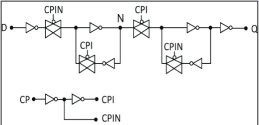
Recently, Stojanovic et al. [14] studied the performance of various
DFFs, and they are found the Semi-Dynamic D Flip-Flop (SDDFF)
[4]. The term semi dynamic is used here to denote circuits that
internally have a pre-charge and evaluation phase, similar to dynamic gates. This SDDFF has better performance than the conventional master-slave flip-flop in several conditions. The basic diagram of the (SDDFF), as shown in Fig. 3(a), is to clock
a single 6T transparent true single phase clocked (TSPC) latch,
as shown in Fig. 3(b), with a very narrow pulse to reduce latency.
The signal at node ‘S’ is a delayed and inverted version of CLK when temporarily neglecting the effect of feeding the signal ‘X’
to the NAND gate.
(a)
(b)
Fig. 3: (a) The Semi-Dynamic Flip-Flop, (b) the 6T TSPC
Latch
Then, the net effect of the clock CLK to series to connected MN1 and MN3 is equivalent to applying a locally generated pulse to the circuit. By adding the NAND gate in Figure 3(a), the circuit allows
the reduction of the pulse window by about one inverter delay at the expense of a small space penalty for increased loading on node
‘X’. The operating principle of the SDDFF is described briefly as follows. When the clock signal is at falling edge, the flip-flop is going to pre-charge phase. Node ‘X’ is pre charged to supply
voltage Vdd at that time output node ‘Q’ is cutting off from input stage. So, the output static latch holds previous value. When the
clock is at rising edge, the flip-flop enters into evaluation phase.
The evaluation phase begins with the rising edge of clock CLK. If
input D is low the flip-flop is latching a zero, node ‘X’ will remain
high. In this situation the output node ‘Q’ either will remain low
or will be discharged through transistors MN4-MN5. If input D were high prior to evaluation phase the flip-flop is latching one node ‘X’ would be discharged through the pull down path MN1-MN3. The falling transition of ‘X’ would turn transistor MP2 ON,
driving output ‘Q’ high.
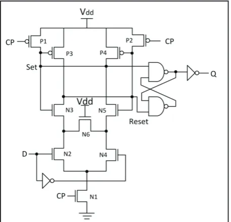
III. Proposed True Single Phase Pulse Clocked D Flip-Flop
The idea of the pulsed triggered clock signal has been applied
to design of the Pulse Triggered TSPC flip-flop [PTTFF]. This PTTFF develop from the TSPC split output D latch with better
speed performance and less area consuming. The main advantage
of the PTTFF is that it has less number of clocked MOS devices.
So, the power consumption of the clock network can be reduced
correspondingly. The true single phase pulse clocked D flip-flop shown in Fig. 4(a), with less number of transistors are used to design with two transistors are being clocked. This new DFF
developed from the conventional TSPC split output D latch is
shown in Fig. 4(b). This new DFF is also similar to the semi dynamic DFF.
The operation of the new DFF is explained below. The input data
are ready to start before rising edge of the clock. When the clock
pulse (CLK) is zero, then pull down transistor MP1 is turned ON to the pre-charged node ‘P’. Now, the pull down transistor MN1 is ON because of the high level logic value at node ‘S’ and node ‘Q’ will be pre-charged. When the clock is going to high, transistor MN2 will be ON state. The pull down transistor MN1 is still ON for a moment before the falling edge of the inverted
(a)
(b)
Fig. 4: (a) Proposed True Single Phase Pulse Clocked DFF and (b) TSPC Split-output D latch
When CLK is ‘0’ and if D is ‘1’, transistors MP1 is turned OFF and MN3 is turned ON. Now, node ‘R’ will be pre-discharged. When CLK goes high, transistors MN1-MN3 are turned ON simultaneously for a short time. Nodes P, Q, and R will be discharged very soon to turn ON transistor MP2. When the falling edge at node ‘S’ arrives, MN1 will be turned OFF and the output
‘0’ enters the latched state.
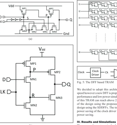
High speed matrix calculations are needed in high Performance
graphic and DSP ICs. The transposition memory (TRAM) is one of
the most important matrix processing blocks. Because of the high
speed demand for future real time systems, TRAM is required to work as fast as possible. The high speed TRAM is developed by using DFF architecture. This DFF is developed from the true single phase pulse clocked split output D latch. The DFF based TRAM is shown in Fig. 5 [15]. This DFF based TRAM can fulfill the
performance demand in high speed or real time DSP applications. The data is shifted from left to right and top to bottom. This
TRAM performs transposition on the fly and eliminates the need
for double buffering, which would have been necessary had a
static dual addressed RAM being used. The maximum operating
frequency is only the inverse of the delay time sum of these two components. Improve the Performance of these two components
will have a definite impact on the overall performance.
Fig. 5: The DFF based TRAM
We decided to adopt this architecture for the purpose of high
speed however a new DFF is proposed to achieve both high speed
performance and low power simultaneously. The operating speed
of this TRAM can reach above 250MHz. The power dissipation of the design using the proposed DFFs is less than that of the design using the SDDFFs. The total power saving is 37.6%. The power saving of the clock driver and DFFs dominate the overall
power saving.
IV. Results and Simulations
The proposed, new true single phase clocking technique based D
flip-flop is compared with the conventional single edge triggered flip-flops to get their performance Metrics. Here two conventional edge triggered flip-flops are designed, namely DISAFF and SDFF. The target technology is 45nm CMOS and the process is
implemented in Virtuoso Schematic Editor and Spectre Simulator. These tools are part of Cadence Virtuoso Design Environment provided by Cadence Design Systems. Generic Process Design
Kit (GPDK) 45nm technology file is used to get the transistor models. The operating conditions for simulation are 10MHz to 250MHz and supply voltage is 1V. The simulation set up model of proposed technique shows Fig. 6. In this set up model the data buffers power consumption, loading effect of the flip-flop and previous stage is also included. The flip-flop has load capacitance of value 20fF capacitor and an extra capacitance after the clock buffer is also placed with a value of 3fF.
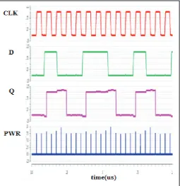
To analyze the performance of the proposed work Fig. 7 shows the
simulations wave form of the proposed true single phase clocked D
flip-flop. Table 1 summarizes some important performance metrics of the various single edge PTDFF designs. These include transistor
count, minimum D to Q delay average power consumption and
power-delay-product (PDP). Power saving of the proposed flip-flop design against CTGFF and DISAFF are 94% and 78% respectively for 100% switching activity. The CTGFF consumes more power than proposed a D flip-flop consumes less power.
Fig. 7: Proposed Flip-Flop Design Simulation Results
To get, more practical performance, the general power consumption
for different input patterns is simulated. Consider five different
data progression to represent various input switching actions. The sequence of …010101… represents 100% switching activity, 00110011… represents 50% switching activity, and … 00010001… represent 25% switching activity. Two other sequences …11111… and …00000… are used to represent the switching activity of 0%.
We compare the power consumption and power-delay-product at 100% switching activity with conventional edge triggered flip-flop designs.
Table 1: Data Performance Metrics Comparison of Various Single Edge PTFF
Type of Flip-Flop TGFF DISAFF SDFF Proposed Design D
Flip-Flop
Transistors 24 21 15 12
Maximum D-to-Q
delay(ns) 7.05 5.55 2.33 1.60
Average power µW
(100% Activity) 2.03 0.50 0.14 0.11
Power-Delay-
Product(fJ) 14.72 2.82 0.32 0.180
Table 2: Data Switching Activity Comparison of Various Single Edge PTFF
Type of Flip- Flop TGFF DISAF-F SDFF Proposed Design D
Flip-Flop
Average Power µW
(100% Activity) 2.031 0.509 0.141 0.112
Average Power µW
(50% Activity) 1.813 0.410 0.072 0.050
Average Power µW
(25% Activity) 1.811 0.383 0.063 0.048
Average Power µW
(0% Activity,all-1) 1.025 0.321 0.055 0.046
Average Power µW
(0% Activity,all-0) 1.023 0.313 0.051 0.039
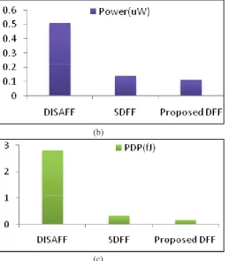
Table 3: Performance Comparisons of TRAM by Using Conventional and Proposed Flip-Flops
Types of
TRAM Voltage (V) Temperature (°C) Power(µW) Delay(ns) PDP(fJ)
SDFF 1 27 55.7 0.47 26.34 DISAFF 1 27 39.0 5.10 199.4 Proposed
DFF 1 27 34.7 5.10 177.1
Fig. 9: Data Switching Activity Comparison of Various Single Edge PTDFF
(b)
(c)
Fig. 10: Power (a) Delay (b) PDP(c) Comparisons of Conventional Flip-Flop and Proposed D-FF
V. Conclusion
In this paper, a low power single edge pulse triggered flip-flop
is designed based on a true single phase clocked technique. Simulation results and performance metrics such as an average
power and minimum D-to-Q delay and PDP indicate that the proposed pulsed flip-flop design is more efficient compare to conventional master-slave flip-flop design. The proposed design
is reduced 91% power and 77.2% delay and 98.2% PDP at 100%
data activity as compared to CTGFF. It is suitable for design
of high performance embedded memory architectures with low power consumption.
References
[1] H. Kawaguchi, T. Sakurai,“A reduced clock-swing flip-flop (RCSFF) for 63% power reduction,” IEEE Journal Solid-State Circuits, Vol. 33, No. 5, pp. 807-811, May 1998. [2] F. Klass, C. Amir, A. Das, K. Aingaran, C. Truong, R. Wang,
A. Mehta, R. Heald, G. Yee,“Semi-dynamic and dynamic flip-flops with embedded logic,” In Symp. VLSI Circuits, Tech. Dig. Papers, 1998, pp. 108-109.
[3] J. Yuan, C. Svensson,“High-speed CMOS circuit technique,” IEEE J. Solid-State Circuits, Vol. 24, No. 1, pp. 62-70, February 1989.
[4] F. Klass, C. Amir, A. Das, K. Aingaran, C. Truong, R. Wang, A. Mehta, R. Heald, G. Yee,“A new family of semi dynamic and dynamic flip-flops with embedded logic for high performance processors,” IEEE J. Solid-State Circuits, Vol. 34, No. 5, pp. 712-716, May 1999.
[5] J. Shinde, S.S.Salankar,“Clock gating - A power optimizing technique for VLSI circuits”, IEEE India Conf. 2011 Annual IEEE. (2011) pp. 1-4.
[6] X. wang, W.H. Robinson,"A low-power double edge-triggering flip-flop with transmission gates and clock gating", Proc. MWSCAS (2010) pp. 205-208.
[7] G. Gerosa,“A2.2W, 80 MHz superscalar RISC microprocessor,” IEEE Journal Solid-State Circuits, Vol. 29, No. 12, pp.
1440-1454, Dec. 1994.
[8] U. Ko, P.Balsara,“High performance energy efficient D flip-flop circuits,” IEEE Trans. Very Large Scale Integra. (VLSI) Systems, Vol. 8, No.1, pp. 94-98, Feb. 2000.
[9] B. Nikolic, V. G. Oklobzija, V. Stojanovic, W. Jia, J. K. Chiu, M. M. Leung,“Improved sense-amplifier-based flip-flop: Design and measurements,” IEEE Journal Solid-State Circuits, Vol. 35, No. 6, pp. 876-883, Jun. 2000.
[10] S. D. Naffziger, G. Colon-Bonet, T. Fischer, R. Riedlinger,
T. J.Sullivan, T. Grutkowski, “The implementation of
the Itanium 2 microprocessor,” IEEE Journal Solid-State Circuits, Vol. 37, No. 11, pp. 1448-1460, Nov. 2002. [11] N. Weste, D. Harris,“CMOS VLSI Design”, Reading, MA:
Addison Wesley, 2004.
[12] J. Rabaey, A. Chandrakasan, B. Nikolic,"Digital Integrated Circuits", 2nd ed. Englewood Cliffs, NJ: Prentice-Hall, 2003.
[13] A. Chandrakasan, W. Bowhill, F. Fox,"Design of High Performance Microprocessor Circuits", 1st ed. Piscataway, NJ: IEEE, 2001.
[14] V. Stojanovic, V. Oklobdzija,“Comparative analysis of master-slave latches and flip-flops for high-performance and low-power systems,” IEEE Solid-State Circuits, Vol. 34, No. 4, pp. 536-548, April 1999.
[15] T. Xanthopoulos, A. Chandrakasan,“A low-power IDCT Macrocell for MPEG-2 MP@ML exploiting data distribution properties for minimal activity,” IEEE J. Solid State Circuits, Vol. 34, No. 5, pp. 693-703, May 1999.
G.Brahmaiah received his Bachelor's
degree in Electronics and
Communic-ation Engineering from AVR & SVR College of Engineering and Technology,
Nandyal, India, in 2013 and pursuing his Master’s degree in Digital Electronics
and Communication Systems from Vardhaman College of Engineering (Autonomous), Hyderabad, India. His research interests include low power
CMOS VLSI technology.
S. Rajendar received his Bachelor’s
Degree and Master’s Degree from Jawaharlal Nehru Technological University, Hyderabad. He is currently pursuing his Ph.D from JNTU,
Hyderabad. At present he is working as Associate Professor, ECE at Vardhaman College of Engineering (Autonomous), Hyderabad. He is having 12 years of teaching experience. He is a member
of IEEE, IETE, ISTE, SAISE, IAENG, UACEE, and IACSIT. He has more than
20 research publications in national and international conferences
and journals to his credit. His research interests include
High-performance Low Power VLSI circuit design, Interconnect
C. Lokanath Reddy received his
Bachelor’s Degree and Master’s Degree
from Sree Visveswaraya Institute of
Technology, Mehboobnagar, India.
He is presently working as Assistant Professor in the department of ECE, Vardhaman College of Engineering (Autonomous), Hyderabad, India. He
is a member of IETE, SAISE, IAENG and UACEE. His research interests include Analog and Mixed Signal