University of South Carolina
Scholar Commons
Theses and Dissertations
2013
Accuracy, Cost and Performance Trade-Offs for
Streaming Set-Wise Floating Point Accumulation
on FPGAs
Krishna Kumar Nagar
University of South CarolinaFollow this and additional works at:https://scholarcommons.sc.edu/etd Part of theComputer Engineering Commons
This Open Access Dissertation is brought to you by Scholar Commons. It has been accepted for inclusion in Theses and Dissertations by an authorized administrator of Scholar Commons. For more information, please [email protected].
Recommended Citation
Accuracy, Cost and Performance Trade-offs for Streaming Set-wise
Floating Point Accumulation on FPGAs
by
Krishna Kumar Nagar
Bachelor of Engineering
Rajiv Gandhi Proudyogiki Vishwavidyalaya 2007
Master of Engineering University of South Carolina 2009
Submitted in Partial Fulfillment of the Requirements
for the Degree of Doctor of Philosphy in
Computer Engineering
College of Engineering and Computing
University of South Carolina
2013
Accepted by:
Jason D. Bakos, Major Professor
Duncan Buell, Committee Member
Manton M. Matthews, Committee Member
Max Alekseyev, Committee Member
Peter G. Binev, External Examiner
Dedication
Dedicated to
Acknowledgments
It took me 6 years, 2 months and 27 days to finish this dissertation. It involved the
support, patience and guidance of my friends, family and professors. Any words of
gratitude would not be sufficient for expressing my feelings.
I would like to thank my committee members Dr. Duncan Buell, Dr. Manton
Matthews, Dr. Max Alekseyev and Dr. Peter Binev. Their guidance, suggestions
and feedback at various instances has greatly benefited this work and my knowledge.
I would also thank them for patiently reading this document and be approving of this
research.
It would have been impossible for me to pursue the research without the guidance
and instruction of Dr. Jason Bakos. He not only has been supportive but also
encouraging. His dedication, commitment and enthusiasm kept me motivated and
inspired. Foremost, he has been patient with me throughout. I cannot imagine a
better mentor, guide and adviser for my PhD.
I would like to express my gratitude towards my colleges in the Heterogeneous and
Reconfigurable Computing Lab especially Zheming Jin and Yan Zhang with whom I
worked on various projects. I would also thank Ibrahim Savran, with whom I prepared
for the qualifying exam and had discussion on various many research topics.
My family has always provided me unconditional support and have always kept
Abstract
The set-wise summation operation is perhaps one of the most fundamental and widely
used operations in scientific applications. In these applications, maintaining the
ac-curacy of the summation is also important as floating point operations have
inher-ent errors associated with them. Designing floating-point accumulators presinher-ents a
unique set of challenges: double-precision addition is usually deeply pipelined and
without special micro-architectural or data scheduling techniques, the data hazard
that exists. There have been several efforts to design floating point accumulators
and accurate summation architecture using different algorithms on FPGAs but these
problems have been dealt with separately. In this dissertation, we present a general
purpose reduction circuit architecture which addresses the issues of data hazard and
accuracy in set-wise floating point summation. The reduction circuit architecture
is parametrizable and can be scaled according to the depth of the adder pipeline.
Also, the dynamic scheduling logic we use in this makes it highly resource efficient.
Further, the resource requirements for this design are low. We also study various
methods to improve the accuracy of summation of floating point numbers. We have
implemented four designs. The reduction circuit architecture serves as the framework
for these designs. Two of the designs namely AEC and AECSA are based on
com-pensated summation while the two designs called EPRC80 and EPRC128 implement
set-wise floating point accumulation in extended precision. We present and compare
the accuracy and cost- operating frequency and resource requirements- tradeoffs
as-sociated with these designs. On the basis of our experiments, we find that these
and EPRC128– operate at around 180MHz on Xilinx Virtex 5 FPGA which is
com-parable to the reduction circuit while AECSA operates at 28% less frequency. The
increase in resource requirement ranges from 41% to 320%. We conclude that
accu-racy can be achieved at the expense of more resources but the operating frequency
Table of Contents
Dedication . . . iii
Acknowledgments . . . iv
Abstract . . . v
List of Tables . . . ix
List of Figures . . . x
Chapter 1 Introduction . . . 1
Chapter 2 Background . . . 5
2.1 Field Programmable Gate Array . . . 5
2.2 Floating Point Representation- IEEE-754 Standard . . . 5
2.3 Floating Point Addition . . . 7
Chapter 3 Previous Work. . . 12
3.1 Methods to Improve Accuracy of Floating Point Summation . . . 12
3.2 Set-wise Floating Point Summation on FPGAs . . . 20
Chapter 4 Preliminary Work . . . 25
4.1 Reduction Circuit Architecuture . . . 27
Chapter 5 Research Implementation . . . 36
5.1 Custom Floating Point Adder with Error Output . . . 38
5.3 Adaptive Error Compensation in Subsequent Addition . . . 48
5.4 Extended Precision Reduction Circuit . . . 56
5.5 Summary of Designs . . . 59
Chapter 6 Experiments and Results . . . 61
6.1 Resource Requirements and Operating Frequency . . . 61
6.2 Accuracy . . . 67
Chapter 7 Conclusion and Future Work . . . 76
7.1 Conclusion . . . 76
7.2 Future Work . . . 78
List of Tables
Table 2.1 Round To Nearest . . . 9
Table 3.1 Mean Square Errors for Different Orderings . . . 14
Table 3.2 Comparison of Different Reduction Circuits . . . 24
Table 6.1 Custom Floating Point Adder . . . 62
Table 6.2 Number of Comparisons for Designs . . . 65
Table 6.3 Resource Requirements and Operating Frequency . . . 66
Table 6.4 Erroneous Bits for κ= 1.0 and Varying Exponent Difference . . . . 71
Table 6.5 Erroneous Bits for κ=∞ and Varying Exponent Difference . . . . 71
Table 6.6 Erroneous Bits for Varyingκ and Exponent Range = 0 . . . 72
Table 6.7 Erroneous Bits for Varyingκ and Exponent Range = 32 . . . 73
Table 6.8 Relative Errors for Sparse Matrices . . . 75
List of Figures
Figure 2.1 Binary Interchange Format . . . 6
Figure 2.2 Floating Point Addition Algorithm . . . 8
Figure 2.3 Non-associativity of Floating Point Addition . . . 11
Figure 3.1 Error Free Transformation- Error Recovery . . . 16
Figure 4.1 Accumulators . . . 26
Figure 4.2 Reduction Circuit Components . . . 28
Figure 4.3 Reduction Circuit Rules . . . 31
Figure 4.4 Tracking Set ID . . . 33
Figure 4.5 Reduction Circuit Module . . . 35
Figure 5.1 Fast2Sum Algorithm in Hardware . . . 39
Figure 5.2 Rounding Error due to Round and Shift . . . 42
Figure 5.3 Custom Floating Point Adder with Error Output . . . 43
Figure 5.4 Error Accumulation and Compensation . . . 46
Figure 5.5 Module for Error Accumulation and Compensation . . . 47
Figure 5.6 Error Compensation in Subsequent Addition . . . 49
Figure 5.7 Adaptive Error Compensation in Subsequent Addition . . . 50
Figure 5.8 Module for AECSA . . . 51
Figure 5.9 Working of Four Counters in AECSA-ERC . . . 54
Figure 5.10 Extended Precision Reduction Circuit . . . 57
Chapter 1
Introduction
The floating point summation operation– or accumulation–, S =
n
X
i=1
ai is one of the
most widely used operations in scientific applications such as computational fluid
dynamics, structural modeling, power networks and it also forms the core of most of
the basic linear algebra subroutines(BLAS)[39]. In a simplistic scenario, accumulation
can be performed using the following snippet of code:
f o r( i = 1 ; i < n+1; i ++) {
S = S + a [ i ] ;
}
In many applications, like sparse matrix vector multiplication, it is required to
accumulate streaming datasets of different sizes. The applications also require high
numerical accuracy. Achieving high performance for the accumulation operation
presents two challenges. Firstly, on a parallel computer, the summation can be
per-formed using a parallel “reduction” operation. In this operation, multiple additions
are performed concurrently, producing multiple “partial” sums that are maintained
separately until they are eventually added into a final result. The problem with this
approach is that since floating point addition is not associative and different orders in
which the additions are performed lead to different rounding errors. This means that
the error encountered during the reduction is associated with its runtime behavior.
The second challenge arises from the fact that floating point adders are deeply
pipelined. If a new input is delivered to the adder every clock cycle, it cannot
hazard. In such a case, the designer cannot use a simple feedback-based accumulator
as it may result in addition of values belonging to different sets. In order to
accu-mulate multiple sets of different sizes and deal with data hazard, a special circuit
with proper scheduling techniques around floating point adders is required. This
re-quirement leads to control overhead which may require additional resources and may
reduce the hardware utilization.
Implementing parallel reduction operations on FPGAs provides some unique
op-portunities to maintain and improve the accuracy and resolve the issue of data hazard.
A rich set of tradeoffs can be made between error bound and resource usage through
the design of customized floating point units. Also, very fine-grained control logic
can be used to reduce the overheads of data dependent behavior.
Several methods have been developed and studied in order to improve the accuracy
of summation. Some of these methods rely on the ordering of the values in the
dataset. These methods require a priori knowledge of the dataset according to which
the dataset can be sorted. Methods have also been developed in which the error
during addition is extracted using floating point operations. This error is incorporated
in the summation results. Another way to improve accuracy is to perform all the
intermediate calculations in extended precision which mitigate the effect of shift and
round operations by proving more guard bits during addition. Some of the accuracy
improving techniques have also been implemented on FPGA based coprocessors. Also,
there have been several efforts to implement streaming set-wise reduction on FPGAs.
All the methods to improve accuracy come at the cost of increased number of
operations. Techniques which require reordering the inputs are not practical for
im-plementation on FPGAs as the upfront cost of reordering is very high which affects the
overall throughput adversely. Also, these methods are not suitable where streaming
datasets are used as reordering the dataset is not possible. Other methods in which
point operations to extract the error and hence the latency can be large.
Perform-ing intermediate calculations in extended precision requires wider and deeper adder
unit. Also, conversion units are required to convert the input to extended precision
and output to native precision format. Methods which rely on error extraction and
compensation as well as those in which extended precision is used are comparatively
less expensive than reordering as dataset need not be pre-processed. Also, a priori
knowledge of the dataset is not required.
The motivation of this research arises from the observation that previous works
ad-dress the problem of improving accuracy and streaming set-wise reduction of floating
point values separately. In this dissertation, we present a high performance general
purpose reduction circuit which addresses the issue of data hazard and scheduling
associated with set-wise floating point accumulation. This reduction circuit achieves
nearly 100% utilization regardless of the structure of the input dataset. We also
ex-amine methods to leverage custom hardware in order to place tighter error bounds on
the accumulation operation. On the basis of our analysis, we have implemented four
designs for accurate summation of set-wise data. Our reduction circuit architecture
serves as the basic framework for these designs. Two of the designs are based on
com-pensated summation methods while in two designs we perform all the intermediate
operations in extended precision.
In compensated summation methods, additional floating point operations are
re-quired which essentially increase the overall latency of the adder network. Due to
the increased latency, additional resources are required to store the partial sums and
the control logic becomes complex. In order to reduce the number of floating point
operations, we have designed a custom floating point adder which not only adds two
input values but also produces the rounding error which occurs during the floating
point addition. The designs in which we emulate compensated summation methods,
We analyze these designs and evaluate these in terms of accuracy, cost and
perfor-mance. Though, we require more resources for all these designs, but we observe less
impact on the overall performance in terms of operating frequency. We also report
and compare the accuracy of results from simulation of these designs with
simula-tion of original reducsimula-tion circuit and software model of extended precision recursive
summation. We conclude that new designs achieve better accuracy than the original
reduction circuits and simple recursive summation method.
The rest of the document is organized as follows: The Chapter 2, we introduce
FPGAs, IEEE-754 floating point standard and floating point addition. In Chapter 3,
various methods to improve accuracy of floating point summation and
implemen-tations on FPGAs and implemenimplemen-tations of set-wise accumulation of floating point
values have been studied. Chapter 4 describes the design our reduction circuit. In
Chapter 5, we present the implementation details of the new designs for improving
the accuracy of set-wise floating point summation. In Chapter 6, we discuss the
ac-curacy parameters based on our experiments and the tradeoffs associated with the
designs.In Chapter 7, we summarize the dissertation, and discuss the conclusion and
Chapter 2
Background
2.1 Field Programmable Gate Array
Field programmable gate arrays (FPGAs) are configurable logic devices which
con-sist of arrays of configurable logic blocks (CLBs) connected through programmable
interconnects. Modern FPGAs also consist of hardwired logic blocks such as RAMs
and DSPs. Application specific logical functions can be implemented and updated
on these devices.
In reconfigurable computing, kernel computations are performed using special
purpose architectures that are implemented on one or more FPGAs. Designs on
FP-GAs generally achieve better performance than software implementations on general
purpose processors because as every hardware component is dedicated to the
compu-tation. It is similar to designing application specific integrated circuits (ASIC) except
that the resultant frequency on FPGA(s) is about 10x slower than ASICs.
2.2 Floating Point Representation- IEEE-754 Standard
IEEE-754 floating point standard has been developed in order to simplify the
arith-metic algorithms designed for floating points[16]. The standard has been widely
adopted and thus it ensures interoperability and portability of algorithms on
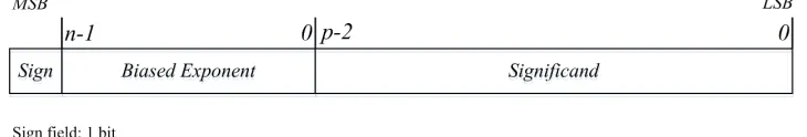
differ-ent machines. The represdiffer-entations are characterized by base(β), precision(p) and exponent range. It allows representation of floating point numbers using base 2
Figure 2.1: Binary Interchange Format
are widely used while the support other formats is still limited.
In IEEE-754 binary formats, apart from special cases, the digit to the left of
the binary point is 1 which is often referred as leading one. This notation is called
normalized form. Figure 2.1 depicts the encoding for a floating point number in the
binary standard. It is called the binary interchange format in which each number has
only one encoding. It has three fields- sign, exponent and significand. The leading
one is not included but is implied in calculations. Also, in order to simplify operations
for exponents like comparison, a bias is used such that the exponent can be treated
as an unsigned integer.
A floating point number A encoded in IEEE-754 format can be calculated as
ˆ
A= (−1)Sign×(1 +Signif icand)×2(Exponent−Bias). (2.1)
where ˆA is the floating point representation of A. Since the number of digits or bits used for representing a fraction is fixed and limited, all numbers cannot be represented
exactly in these formats. Thus the encoding of a number in floating point format its
approximation to the nearest floating point number. That is why floating point format
is often termed as limited precision floating point format as well. For example,
Apart from these standard formats, in order to increase the precision, IEEE-754
also allows extended precision format in which the precision and range of exponent
is defined by the user.
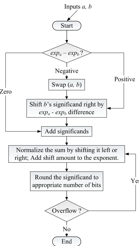
2.3 Floating Point Addition
A number of steps are involved in addition of two floating point values[21, 36]. The
implied one, not included in the representation, is also taken into account. Flowchart
in figure 2.2 depicts the algorithm for addition of two floating point numbers.
First, the exponents of the values are compared. If the exponent of the first input
is smaller then the operands are swapped so that the following shift operation is
restricted in one path of the hardware unit. Then the significand of number with
smaller exponent aligned is with the other significand and the significands are added.
The result is then normalized by shifting it either to left or right and the shift amount
is added or subtracted from the exponent. The resultant is rounded so that it can
be put back in the standard format. Rounding is used to represent the result in
the nearest possible floating point format. Multiple iterations may be required to
round the result properly as the rounded result may require normalization. When
implementing this floating point addition in hardware, extra bits can be used in
order to improve the accuracy. IEEE-754 standard supports various rounding modes
such as round-ties-to-even, round-ties-to-away, positive,
round-toward-negative and round-toward-zero. In this dissertation, we only consider
round-ties-to-even as the methods we use work only with round-to-nearest mode. The reasons have
been explained later.
During floating point addition, extra bits namely guard (G), round (R) and sticky
(S) are used to perform addition of mantissas. Guard bit is the 2nd, round bit is the
1st and sticky bit is the 0th bit in the extended mantissa. In round-to-nearest mode,
Figure 2.2: Floating Point Addition Algorithm
andG,Rand Sbits. The direction of rounding- round-up or round-down- is decided
as depicted in Table 2.1.
It can be observed that whenG is 0, sum is rounded down i.e. towards zero. IfG
is 1, thenRand S are also considered in the rounding decision. Lis only considered
in case of a tie i.e. when G=1, R=0 and S=0, L, otherwise it is in “don’t care” (X)
state.
Table 2.1: Round To Nearest
L G R S Round
X 0 X X Roun Down
X 1 0 1 Round Up
X 1 1 0 Round Up
X 1 1 1 Round Up
0 1 0 0 Round Down (Tie)
1 1 0 0 Round Up (Tie)
implemented as deeply pipelined hardware unit where each step may take one of more
clock cycle for completion. Thus, the latency of a floating point adder is more than
one cycle.
2.3.1 (In)Accurate Floating Point Addition
Methods, in which large floating point datasets are used, may deliver wrong results
due to different sources of errors. Stability of numerical algorithms is an important
topic of research in the field of numerical analysis and much of the focus has been
given to the accuracy of floating point operations [1, 2, 3].
Rounding errors, also called round-off errors, are unavoidable due to prevalence
of finite precision floating point arithmetic[12]. Rounding error can be introduced in
two ways- shift and carry. The error due to shift operation of smaller operand during
addition causes shifting error. A nonzero carry which results the significand width to
be more than the allowed bits causes carrying error.
Real numbers are represented as the nearest possible approximation to a floating
point representation but floating point operations are performed as if the intermediate
results are correct to infinite precision and then rounded for the given format. Thus
the error in a floating point operation involving two numbers can be calculated using
the following equation.
f l(aKb) = (1 +ε)(a·b), |ε|6, = 1 2β
where fl(a J
b) is a floating point operation J ∈ {⊕
, ,⊗, } equivalent to the exact operation · ∈ {+,−,×, / } and β is the base. This is the standard model for numerical error analysis attributed to Wilkinson[19]. is called machine precision or unit roundoff. It gives an upper bound for relative error due to rounding in floating
point arithmetic. It is 2−24 for single precision and 2−53 for double precision.
Equation 2.2 is true only for rounding to nearest rounding mode. In this rounding
mode,
2.3.2 Rounding Error in Summation
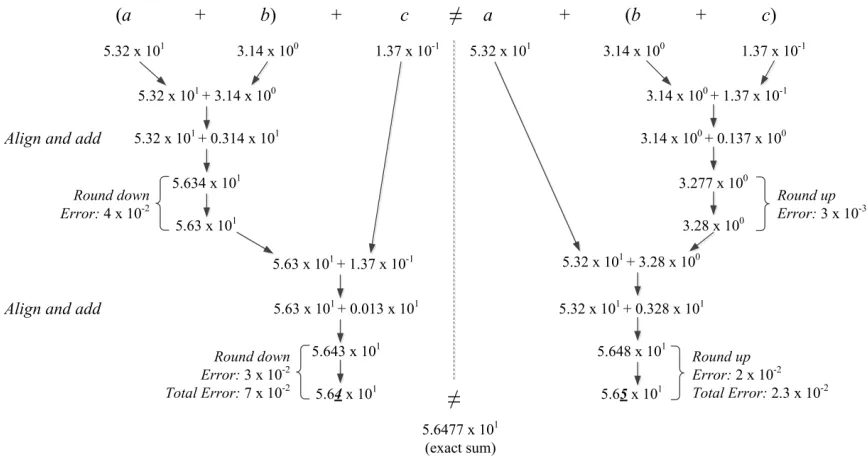
As the number of additions increase, the total error in the result also increases.
As shown in figure 2.3, floating point addition is not associative hence each of the
possible orderings may produce a different summation and the corresponding error
may vary greatly as well. Conversely, the summation calculated in one way may be
more accurate than the summation calculated in another way. The error bound for
recursive summation is given by the following equation[2]:
|En|6(n−1) n
X
i=1
|ai|+O(2) (2.3)
This error bound has been deduced by taking into consideration the error
intro-duced in each iteration step of the recursive addition and thus is dependent on the
number of terms being added. It is independent of the order in which the values are
added. In order to reduce the error in the result, the input values can be reordered
such that the final summation is more accurate and the error bound given by the
equation is minimized.
Given a set ofnnumbers, the number of ways in which they can be added is given
by:
Cn =
1 (n+ 1)
2n n
!
= (2n)!
Figure 2.3: Non-associativity of Floating Point Addition
whereCnis called the Catalan number. Since this number grows very large even with
small number of values, it is not possible to try every possible ordering and choose
Chapter 3
Previous Work
In this chapter, we summarize various methods to improve accuracy of floating point
summation, implementations of these methods on FPGAs and implementation of
set-wise floating point summation on FPGAs.
3.1 Methods to Improve Accuracy of Floating Point Summation
In this section, we discuss different methods to improve accuracy. First, we discuss
the dependence of error bounds and relative error on the distribution of value in
a dataset. Then, we explain the effects of reordering the data on the summation
error. Then we discuss the methods in which the error encountered during floating
point addition is calculated and incorporated into the final summation. We also
present a method in which extended precision is used to improve the accuracy of the
intermediate operations.
3.1.1 Relative Error and Condition Number
In numerical error analysis, the error bounds are derived as if the worst case error
occurs always and is propagated throughout the computation. For this to happen,
rounding during all intermediate operations should be in same direction. In general,
the rounding direction is random and the errors often cancel out each other. Thus
the magnitude of final error can be very small. Also, the magnitude of error also
depends on the order of values being added. Hence, the relative error with respect
error. The relative error is the ratio of the error,|En| and the summation calculated
with infinite precision as depicted in equation 6.2. In this equation, the error, |En|
is the difference between the exact summation calculated with infinite precision, |Sn|
and the recursive summation in floating point precision, Sn.
|En| |Sn|
= |Sn| −Sn
|Sn|
(3.1)
The ratio of summation of absolute values and the recursive summation denotes
the condition number, κ, of the dataset and is calculated as in equation 6.1.
κ= Pn
i=1|ai| |Pn
i=1ai|
(3.2)
If a dataset consists of only positive values then κ = 1.0 while κ > 1.0 denotes that the dataset consists of both positive and negative values. The relative error
bound of summation methods is proportional toκ. If κ1.0, the relative error can be large even for methods used for achieving high accuracy. Thus, a low error bound
does not always lead to low relative error.
3.1.2 Reordering Inputs to Achieve Better Accuracy
In floating point summation, the error in final result has been attributed to several
factors. Catastrophic cancellation occurs when the final result is much smaller than
the intermediate sums. It is due to the presence of large intermediate sums with
opposite signs. A method has been proposed in which the numbers are added to
numbers with same sign and the final sum is calculated by adding the result from each
group of numbers. Though this method eliminates the intermediate cancellations, it
results in a cancellation at the end and hence is not effective in error correction.
Large relative errors can also occur when the intermediate results become much
larger than the individual operands. This is caused by the presence of several
Table 3.1: Mean Square Errors for Different Orderings
Distribution Increasing Random Decreasing Insertion Pairwise Uniform(0, 2µ) 0.20µ2n3σ2 0.33µ2n3σ2 0.53µ2n3σ2 2.6µ2n2σ2 2.7µ2n2σ2
Exp(µ) 0.13µ2n3σ2 0.33µ2n3σ2 0.63µ2n3σ2 2.6µ2n2σ2 4.0µ2n2σ2
Note: This is based on the assumption that relative errors in floating point addition are statistically independent and have zero mean and finite varianceσ2. Uniform dis-tribution, Unif(0, 2µ), and exponential distribution, Exp(0,µ) have meanµ.
according to their intervals. Operations can be performed within those intervals and
final result can be calculated by adding results from those intervals[14]. For
distribut-ing the values in intervals and adddistribut-ing the values from different intervals, the values
and summation of intervals can be reordered in different ways to reduce the overall
error.
Several possible orderings have been studied for improving the accuracy of the
summation. It has been observed that if the numbers are added in absolute
ascend-ing order, the error bound is minimized. This results in addition of operands havascend-ing
similar magnitude and hence reduces the carrying error[20]. But if the dataset
con-tains both positive and negative numbers, this method results in a greater error.
Absolute descending order is more beneficial when there is lot of cancellation i.e.
positive and negative numbers are evenly present in the dataset as it reduces the
carrying error.
Another method applicable to positive numbers called the insertion method has
been proposed in which the intermediate partial sum is inserted in the sorted list
of numbers. This is effective in reducing the shifting error but does not work well
for dataset having both positive and negative numbers[6]. In pairwise summation,
operands are added in pairs. This method is suited for parallel implementation with
binary tree of adders. The final result can be calculated in log2n steps as opposed to
n-1 steps required for serial recursive summation at the expense of resources[3, 5].
Table 3.1 lists the mean square errors over uniform and exponential distributions
In the above mentioned methods, certain orderings were considered so as to reduce
the amount of error in the final result. These methods do not calculate or take into
consideration the error which occurs. The input set size and magnitudes have to
be known a priori. Also, these methods require sorting and arrangement of data
which are expensive operations and require more resources. Due to the upfront cost
of sorting the input data, the throughput of the summation is affected adversely.
Further, the error bounds of these methods are data dependent. Thus these methods
are not suitable for high performance implementations.
3.1.3 Compensated Summation
Several methods have been developed where the error during each floating point
ad-dition can be calculated and incorporated into intermediate and the final results[15].
Such methods are categorized as compensated summations. Compensated
summa-tions are based on error free transformation which is a transformation in which
a+b=x+e, x=f l(aMb). (3.3)
Here x is the rounded floating point sum of two floating point numbers a and b
represented in base 2 ande is the error incurred during addition. The errore can be
recovered using floating point operations. During addition, the operand with smaller
exponent,bis shifted by the exponent difference for alignment. The low order bits of
b,bl are discarded. These bits form the error term. Figure 3.1 shows the general idea
behind the recovering bl [1]. Floating point operation,x - a results in high order bits
of b, bh. Subtracting b from bh results in the low order bits of bl. The recovered low
order bits can be incorporated in subsequent additions to get more accurate result.
Algorithm 1 lists Kahan’s compensated summation algorithm which calculates
and applies the correction in each iteration for recursive summation[17]. In this
algorithm, the error terme - the approximation to the rounding error, is subtracted
Figure 3.1: Error Free Transformation- Error Recovery
algorithm in which S + e can be calculated at the end of the loop [18]. It has been
shown that this algorithm improves the error bound and gives almost ideal result.
Equation 3.4 gives the error bound for Kahan’s compensation algorithm which is
independent ofn if n < 1.
|En|6(2+O(n2)) n
X
i=1
|ai| (3.4)
Equation 3.5 gives the relative error bound for Kahan’s compensation algorithm.
|En| |Sn| 6
(2+O(n2)) Pn
i=1|ai| |Pn
i=1ai|
(3.5)
Another version of compensated summation has been developed where the error
terms calculated after each addition are accumulated and the correction is applied
at the end of the summation. The error at each step of recursive addition can be
calculated using Fast2Sum[11] algorithm as depicted in algorithm 2. Algorithm 3
can be used to calculate the final sum. Equation 3.6 shows the error bound for this
algorithm.
|En|6(2+O(n22))
n
X
i=1
|ai| (3.6)
The relative error for this method is given by equation 3.7.
|En| |Sn| 6
(2+O(n22)) Pn
i=1|ai| |Pn
i=1ai|
Algorithm 1 Kahan’s Compensated Summation Algorithm
1: input(a1, a2, ..., an) 2: S =a1
3: e= 0.0
4: for i= 2 :n do
5: if |S|<|ai| then 6: swap(ai, S) 7: end if
8: y=ai−e 9: St=S+y 10: et =St−S 11: e=et−y 12: S =St 13: end for
14: Return(S)
Algorithm 2 Fast2Sum Algorithm
1: Input(a, b)
2: if |a|<|b|then
3: swap(a, b)
4: end if
5: x=a+b
6: bt =x−a 7: e=b−bt 8: Return(x, e)
Algorithm 3 Error Compensation with Fast2Sum
1: Input(a1, a2, ..., an) 2: S =a1
3: e= 0.0
4: for i= 2 :n do
5: (S, ei) =F ast2Sum(S, ai) 6: e=e+ei
7: end for
8: S =S+e
9: Return(S)
Kahan’s compensation method can also be expressed using Fast2Sum as depicted
in algorithm 4.
Algorithm 4 Kahan’s Compensated Summation with Fast2Sum
1: Input(a1, a2, ..., an) 2: S =a1
3: e= 0.0
4: for i= 2 :n do
5: y=ai+e
6: (S, e) =F ast2Sum(S, ai) 7: end for
8: Return(S)
require that |a|> |b|. This essentially creates a branch in software implementations of these algorithms but when implementing these in hardware, the swap operation in
floating point adder eliminates the need of this check and thus accurate summation
can be calculated with three additional steps.
Several other variations compensated summation techniques have been developed
but require significantly more number of floating point operations [4, 7, 8, 9, 10, 35].
It can be observed that in compensated summation methods, additional steps are
required to recover the error encountered during the alignment operation. But these
do not require a priori knowledge of the data hence they are more suitable and less
expensive for hardware implementation.
3.1.4 Intermediate Operations in Extended Precision
Performing the intermediate calculations in higher precision can also be useful in
achieving higher accuracy [22, 23]. For example, on x86 CPUs, the floating point
numbers denoted in single and double precision are converted to 80-bit extended
precision format and the operations are performed in this format. Computations in
extended precision format lead to results at least as accurate as 64-bit results. In
other words, the error in result from extended precision cannot be more than that
from double precision. This is because extended precision format ensures presence of
more guard bits and hence improves the rounding error. The numbers are converted
lead to more accurate results without much impact on the performance.
All the aforementioned methods to improve the accuracy of summation
opera-tions require additional additional operaopera-tions. Methods which require reordering the
dataset need sorting which is a complex task. Compensated summation methods
require additional floating point operations for calculating and incorporating the
er-ror. Wider adder and intermediate storage units are required during calculations in
extended precision. Thus all the methods to improve accuracy come at additional
cost of resources and floating point operations.
3.1.5 Implementation on FPGAs
There have been several attempts to implement the methods which improve the
accu-racy of floating point summation on FPGAs. When designing accurate accumulators,
approaches can be broadly divided in two categories- those that reorder the inputs
to reduce the errors and those that use error free transformations to find and correct
the errors.
In the reordering approach the properties of the set to be accumulated-sign and
magnitude of values and size of the input set- are known a priori in order to
pre-process the data. A group from Texas A&M University designed a custom adder for
accumulation[32]. In this implementation, exponents of all the inputs are compared
and the significands are aligned for the greatest exponent. Then the significands are
added as fixed point numbers. Though this method reduces the error bound, it comes
with the overhead of sorting and storing all the inputs. Also, wide integer addition is
a slow operation, hence width of the aligned significands becomes a limiting factor.
Another approach has been described in [31] to get the same results as in-order
inputs. The sum is calculated using parallel prefix reduction network and verified
after each reduction step. If the addition is not same as in-order sum, the calculated
is achieved. While this leads to the final summation equal to that in original order but
multiple cycles may be required to converge to zero error. Further, static scheduling
is required along with a fixed number of inputs in a set. Also, this does not reduce
the error in the summation operation.
In order to achieve better accuracy in floating point summation, an iterative
distil-lation algorithm involving Fast2Sum for error free transformation was implemented
on FPGAs in [33]. The number of iterations required to achieve the accuracy
de-pends on the number of values and nature of the data in the set. A custom adder was
also developed to reduce the number of floating point operations and dependence on
data set but the resource utilization was reported to be 47% and 121% higher than
Fast2Sum implementation for single and double precision custom adders respectively.
Also, the performance remains the same for single precision and degrades for double
precision. Thus, this approach does not scale well with precision.
The most recent approach to implement accurate summation operation has been
described in [34]. Here, a binary tree network is used for summation. Custom
adders have been used in the binary tree which output the residue error resulting
from the shift operation in addition along with the sum of inputs. These errors are
accumulated using another binary tree and are added to the result emerging from
the main binary tree iteratively. The number of iterations required for convergence
of error are not bound and may vary significantly with data. Also, two binary tree
networks are used and hence the number of resources required are very high.
3.2 Set-wise Floating Point Summation on FPGAs
In large system solvers such as Conjugate Gradient, in which sparse input data is used,
the data is divided into multiple sets and these sets are generally of different sizes. The
input values generally have a DII of one cycle and and sets are not intermixed. We
of summation do not address the issue of data hazard and cannot handle streaming
datasets. In order to accumulate different data sets represented in floating point
values, a special architecture is required which not only is able to handle multiple
sets simultaneously but also addresses the issue of data hazard which occurs due to
deeply pipelined floating point adders. In this section, we discuss such architectures.
There have been several attempts in designing FPGA-based double precision
ac-cumulators for streaming data. These approaches can be broadly divided in two
categories- static scheduling and dynamic scheduling.
3.2.1 Static Scheduling Approach
A notable example of static scheduling approach was presented by deLorimier et
al[30]. Here the input values and partial sum belonging to different sets are interleaved
such that consecutive values belonging to each set are delivered to the accumulator
at a period corresponding to the pipeline latency of the adder. The accumulator
in this case can be designed as a simple feedback adder. This allows the adder to
accept a new value every clock cycle while avoiding the accumulation data hazard
among values in the same accumulation set. Unfortunately, this method requires a
large up-front cost in scheduling input data and is not practical for large data sets.
The requirement of computation and communication scheduling technique makes the
architecture’s performance highly dependent on the structure of the input data. Also
the memory requirement for such designs is high in order to save the partial sums.
3.2.2 Dynamic Scheduling Approach
The second approach is to use a dynamic scheduling technique that selects the input to
the adder in runtime. This requires managing the progress of each active accumulation
set using a controller which manages the input to the adder. Dynamic scheduling
in which the reduction circuit is integrated within custom floating point adder. In
the following sections, we discuss designs based on these two approaches.
3.2.2.1 Reduction Circuit Around Standard Adder
Prasanna’s group at the University of Southern California as written several seminal
papers in this area [24, 25]. Their first design was a collapsed a binary adder tree
organized as a linear series of adders where the number of adders scaled up as a
logarithmic function of the maximum number of expected input values to be
accu-mulated. Each adder in the system saw an exponentially lower utilization than the
adder before it. This design also had a long latency, had to be flushed between input
sets, and the maximum input set size was fixed at design time. As a result, this
design was resource inefficient and had very low adder utilization.
Their follow-up design was based on the notion of using a single adder to coalesce
an accumulation set while another adder begins reading the next input set. This
design required only two adders, but its FIFO would overflow when the size of the
input sets were, on average, less thanαdlog2α+ 1evalues each, whereαis the adder latency. Also, the controller complexity required by this reduced its maximum speed
by nearly 20%, relative to the maximum speed of the floating-point adder that it was
built around.
Their final design overcame this limitation and required only one adder but also
required two memories of size α2 and a control overhead speed reduction of about 3%. Both of these designs had extremely complex controller overhead which limited
their operating speed and effective throughput.
An implementation from UT-Knoxville and Oak Ridge National Laboratory used
the collapsed binary tree approach but with a parallel–as opposed to a linear–array
significantly more resources as it requires multiple adders. Also, the resources are
poorly utilized.
Huang et al[26] present three reduction circuit designs based which also use the
collapsed binary tree approach. The first design- modular fully pipelined architecture
has dlog2αe + 1 adders connected in a chain. There is a buffer associated with each of the adders where the incoming value (first adder) or partial sum from the previous
adder is stored and added to the next value. The last adder has a feedback loop
associated with it. This approach is very similar to a collapsed binary tree of adders
and provides pairwise addition of input values. The utilization ratio of each adder
is reduced at each stage of the chain. Also, the accumulator is allowed to reduce
only one set at a time hence the following sets have to wait for complete reduction
of one set. The second design uses two adders- one as partial sum generator while
the other as accumulator. But it has a chain of FIFOs connected with the first adder
which are used to delay the incoming values so in order to match the latency of the
floating point adder. Role of adder in the accumulator remains the same. The third
design is similar to the AeMFPA but changes the structure of FIFOs used. These
three designs do not allow multiple sets to enter the accumulator stage thus require
chain of adders or FIFOs to compensate for the latency of accumulate operation.
Further the utilization of the adders is not optimal as they remain ideal for several
cycles during the reduction process. Also, the resource utilization is very high due to
the requirement of multiple adders and FIFOs. Thus the overall throughput of the
reduction circuit suffers.
An improved single-adder streaming reduction architecture was later developed at
the University of Twente[28, 29]. This design requires less memory and less complex
control than the designs discussed previously. In this design, the adder is connected
to two deep input and output buffers. The inputs to the adder are governed by a set
Table 3.2 summarizes the some of the above discussed architectures in terms of
resources- adders, buffers and latency. Note that we do not compare resource usage
and performance because these factor vary with the change in platform used for
implementation.
Table 3.2: Comparison of Different Reduction Circuits
Reduction Circuit # Adders Buffer Size Latency
FCBT[24, 25] 2 3dlog2ne 2n + (α-1)dlog2ne
DSA[24, 25] 2 αdlog2α + 1e αdlog2α + 1e
SSA[24, 25] 1 2α2 2α2
Gerards[28, 29] 1 3α + αdlog2αe + 2 2α +αdlog2αe + 1
MFPA[26] α dlog2αe + 1 < n +αdlog2α + 2e
AeMFPA[26] 2 α log2α + 2α < n +αdlog2α + 2e
3.2.2.2 Integrated Reduction with Custom Floating Point Adder
In each of the above discussed work, standard adders (usually generated with Xilinx
Core Generator) have been used as the core of the accumulator. Another approach
is to design a custom adder such that the de-normalization and significand addition
steps have a single cycle latency, which makes it possible to use a feedback without
scheduling. To minimize the latency of denormalize portion, which includes an
expo-nent comparison and a shift of one of the significands, both inputs are base-converted
to reduce the width of exponent while increasing the width of the mantissa[27]. This
reduces the latency of the denormalize while increasing the adder width. Since wide
adders can be achieved cheaply with carry-chained DSP48 components, these steps
can sometimes be performed in one cycle. This technique is best suited for single
Chapter 4
Preliminary Work
In this section we present an approach to overcome the issue of data hazard in set-wise
accumulation of floating point values. Apart from this primary goal, we also focus
on simplifying the control logic and reducing the amount of memory and resources
required in order to achieve high performance. While designing the reduction circuit,
we consider the following set of constraints:
i. Input values are delivered serially, with a data introduction interval(DII) of one
cycle,
ii. output order need not match the arrival order of accumulation sets,
iii. the accumulation sets are contiguous, meaning that the values from different
accumulation sets are not intermixed and there is a set ID associated with each
incoming value, and
iv. the size of the accumulation sets is not known a priori.
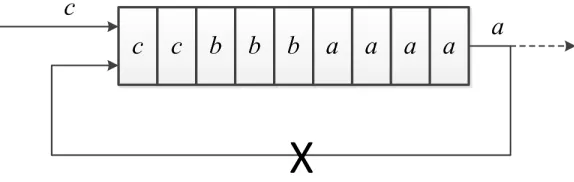
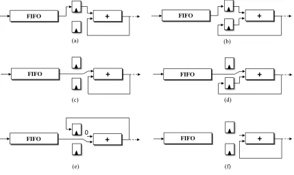
Figure 4.1a shows the design of a simple feedback based accumulator. Since
floating point adder is deeply pipelined and the sum is not available in one cycle,
there exists a hazard as shown in Figure 4.1b. Values belonging to different set may
be added together and hence the results will be wrong. In order to solve this problem,
we can allow just one set to be in the accumulator at any point of time until it is
(a) A Simple Accumulator
(b) Feedback based Accumulator with Pipelined Adder
(c) Reduction Circuit with Scheduling
other incoming sets. Also, the pipeline will be idle for many cycles while its waiting
for the results. Thus, this approach is not only resource intensive but also inefficient.
A special circuit with proper scheduling techniques around floating point adder,
as shown in Figure 4.1c is required. In this chapter, we present a reduction circuit
which is designed around deeply pipelined double precision floating point adder and
addresses the issue of hazard and input scheduling.
4.1 Reduction Circuit Architecuture
The idea behind our reduction circuit design is to expose and exploit parallelism.
Pipelining allows multiple additions within an adder to take place simultaneously. We
also allow accumulation of multiple sets simultaneously. Thus, we exploit both
inter-set and intra-inter-set parallelism. There are various tradeoffs associated with the datapath
design around floating point adder. Depth of the floating point adder pipeline affects
the design parameters such as complexity of control logic, number of buffers required;
i.e., if we increase the depth of the adder, resources-LUTs and registers required on
the FPGA- and the multiplexer fan-in increases, and hence the overall performance
of the circuit in terms of clock frequency goes down. While designing the reduction
circuit we have taken into consideration all these issues.
The reduction circuit has been designed by adding control logic- comparators,
counters, and buffers- around a standard deeply pipelined double precision adder in
order to form a dynamically scheduled accumulator. In this design, we have combined
the input and output buffers and refer them as buffers.
4.1.1 Datapath Components
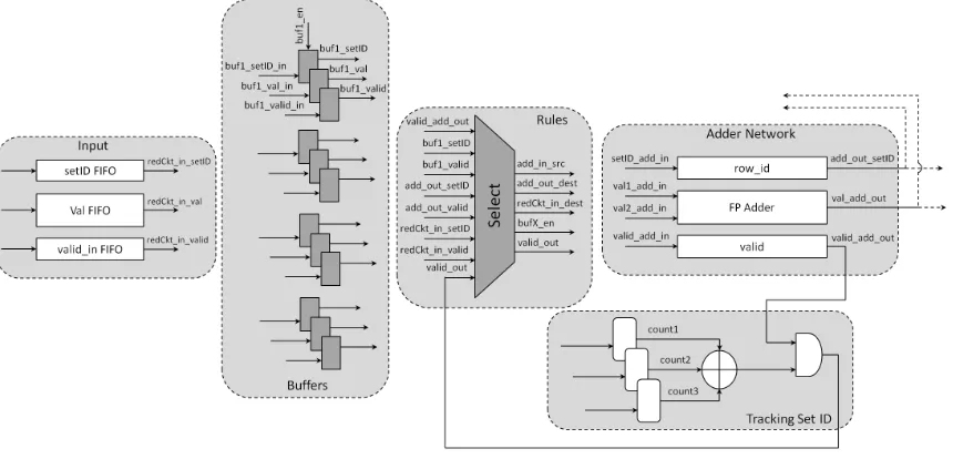
As shown in Figure 4.2, the reduction circuit architecture can be broadly divided
into five interdependent components namely Input, Buffers, Adder pipeline, Counter
Datapath Rules in Control Logic govern the functioning of the other components. In
this section, we describe each of the components.
Figure 4.2: Reduction Circuit Components
In order to describe the rules in a more concise manner, we represent the incoming
input value to the accumulator as input.value and input.set, buffer n as bufn.value
and bufn.set, the value emerging from the adder pipeline as adderOut.value and
adderOut.set, the inputs to the adder pipeline addIn1 and addIn2 and the reduced
accumulated sum as result.value and result.set. Also, we represent the number of
partial sums belonging to set s as numActive(s).
4.1.1.1 Input
The Input component consists of two FIFOs of equal depth- one for the input set ID
and the other for input value. The setID FIFO is 32 bit wide while the Val FIFO is
64 bit wide. The write_enable signals for both the FIFOs are enabled or disabled
simultaneously by external mechanism depending on the supply of input data. The
reduction circuit is supplied the input values along with the respective set ID using
these FIFOs.
4.1.1.2 Buffers
The Buffer component consists of multiple buffer triplets. Each triplet has three
registers- one for set ID (32 bit), one for value (64 bit) and one for valid signal (1 bit)
referred to as buffers. The valid buffer signifies whether the value in the Val buffer is
valid or not. An invalid value is not considered for reduction and can be overwritten.
The buffers are enabled simultaneously for writing. If a value in the triplet is valid,
the triplet can be overwritten only after it has been read. Further, if a valid value
is not available for writing after reading the triplet, the triplet is invalidated. The
bufn.in.validsignal is set by the control logic whilebufn.validsignal is used in control
logic to determine the inputs to the adder where n denotes the triplet number which
we refer to buffer number.
4.1.1.3 Adder Pipeline
The Adder Pipeline consists of two delay lines and a double precision floating point
adder. The set delay line is used for keeping track of the set ID currently in the
floating point adder. The valid delay line checks whether the value in the pipeline
is valid or not. Thus, the set ID propagate through the delay line while the sum is
being calculated. The input to the adder pipeline is decided by Datapath Rules while
the output set ID is used for determining the course of next inputs. The depth of
delay lines is equal to the depth of floating point adder.
4.1.1.4 Datapath Rules
The reduction circuit consists of a set of data paths that allow input values and the
accumulation set ID and the state of the system. Data paths are established by the
control unit according to five basic rules as listed below:
Rule 1: Combine the adder output with a buffered value. Buffer the incoming
value.
Rule 2: Combine two buffered values. Buffer the incoming value. Buffer the adder
output (if necessary).
Rule 3: Combine the incoming value with the adder output.
Rule 4: Combine the incoming value with a buffered value. Buffer the adder output
(if necessary).
Rule 5: Combine the incoming value with 0 to the adder pipeline. Buffer the adder
output (if necessary).
We modeled this behavior of reduction circuit and tested various input
combina-tions for different pipeline latency in order to find the maximum number of buffers
required. We found that for a 14 stage adder, 9 buffers are required such that there
is no overflow and all the sets are reduced correctly. The number of comparisons
required and the fan-in to the adder makes it difficult to place and route the design
and hence we use 4 buffers and an input 32 stage deep FIFO in the reduction circuit.
In order to reduce the number of buffers, we added a special rule which is applied if
all the buffers are occupied and rules 1-5 cannot be applied. The special case is listed
below:
Rule 6: Combine the adder output with 0.
Figure 4.3 shows various configurations of the reduction circuit: a) the output
of the pipeline belongs to the same set as a buffered value; b) two buffered values
set; d) the incoming value and buffered value belong to the same set;e) the incoming
value does not match the set of the pipeline output or any of the buffered values;
f) all the buffers are occupied. Algorithm 5 describes the datapath rules.
Figure 4.3: Reduction Circuit Rules
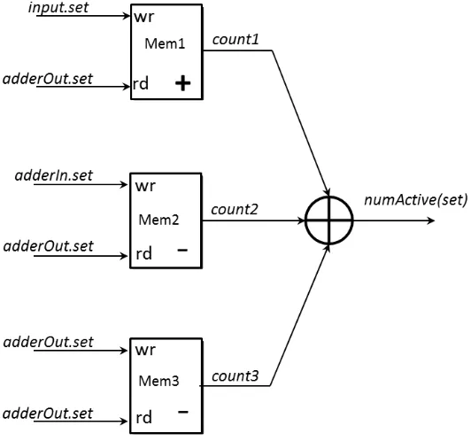
4.1.1.5 Reduction Status of Sets
In order to know when a set has been reduced completely, the entries associated with
the sets must be tracked. Since the number of entries per set is not known a priori
and multiple sets undergo reduction at the same time, we use the corresponding set
ID to track of the entries. We have implemented a counting mechanism which notifies
the control logic if the set coming out of the adder has been reduced completely.
As shown in Figure 4.4, we use three small dual-ported memories, each with a
corresponding counter connected to the write port, in order to determine when a set
ID has been reduced (accumulated) into a single value. Together, these memories
Algorithm 5 Reduction Circuit Rules
1: if ∃n :bufn.set=adderOut.set then .Rule 1 2: addIn1 =adderOut
3: addIn2 =bufn 4: if input.validthen
5: bufn=input 6: end if
7: else if ∃i, j :bufi.set=bufj.set then .Rule 2 8: addIn1 =bufi
9: addIn2 =bufj 10: if input.validthen
11: bufi =input 12: end if
13: if numActive(adderOut.set) = 1 then
14: result=adderOut
15: else
16: bufi =adderOut 17: end if
18: else if input.valid then .Rule 3
19: if input.set=adderOut.set then
20: addIn1 =input
21: addIn2 =adderOut
22: end if
23: else if input.valid then .Rule 4
24: if ∃n:bufn.set=input.set then 25: addIn1 =input
26: addIn2 =bufn
27: if numActive(adderOut.set) = 1 then
28: result=adderOut
29: else
30: bufn=adderOut 31: end if
32: end if
33: else if input.valid then .Rule 5
34: addIn1 =input
35: addIn2 = 0
36: if numActive(adderOut.set) = 1 then
37: result=adderOut
38: else
39: if ∃n:bufn.valid= 0 then 40: bufn=adderOut
41: else
42: ERROR
43: end if
44: end if
45: else .Rule 6
46: addIn1 =AdderOut
47: addIn2 = 0
numActive(). These memories cannot be reset once the reduction circuit has been
activated.
Note that these memories must contain at least n locations, where nis the
maxi-mum possible number of active sets, in order to recycle locations in these memories.
At this time each memory has a depth of 256, which we experimentally verified to be
sufficient for all the datasets that we have tested. Thus, we use the least significant
8 bits of the set ID as input to each of the memories.
Figure 4.4: Tracking Set ID
The write port of each memory is used to increment or decrement the current value
in the corresponding memory location. The write port of one memory is connected to
input.set and always increments the value associated with this set ID corresponding
to the incoming value. Thus, whenever a value belonging to a particular set arrives,
this counter is enabled.
The write port of the second memory is connected to adderIn.set and always
enter the adder. This occurs under all rules except for 5, since each of these rules
implement a reduction operation. Hence, whenever two valid values enter the input
pipeline, this counter is enabled.
As said before, we use the least significant 8 bits of the set ID and the memories
used in the counters cannot be reset and hence, after every 256 set IDs, a memory
location will be reused while the old counter values are still there. In order to
deter-mine correct reduction, we require the third counter. In the third counter, the write
port of the third memory is connected to adderOut.set and always decrements the
value associated with this set ID whenever the number of active values for this set ID
reaches one. In other words, this counter is used to decrement the number of active
values for a set at the time when the set is reduced to single value and subsequently
ejected from the reduction circuit.
The read port of each memory is connected to adderOut.set, and outputs the
current counter value for the set ID that is currently at the output of the adder.
These three values are added to produce the actual number of active values for this
set ID. When the sum is one, the controller signals that the set ID has been completely
reduced. When this occurs, the set ID and corresponding sum is output from the
reduction circuit.
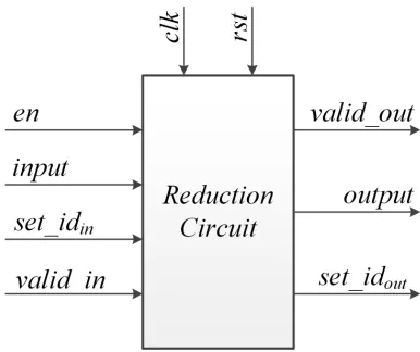
Figure 4.5 shows the reduction circuit module. Apart from the clock and reset
signal, the inputs to the reduction circuit are value (input), set ID (set_idin),valid_in
and an enable (en) signal. The valid_in signal denotes whether the input is valid.
When the en signal is de-asserted, the reduction circuit is disabled and the state
is preserved. This signal facilitates disabling the reduction circuit when the input
stream is discontinued. The outputs of this architecture are the summation of dataset
(output), set ID (set_idout) and a valid_outsignal which denotes whether the output
is valid or not.
Figure 4.5: Reduction Circuit Module
floating point dataset accumulation. This is designed around a deeply pipelined
floating point adder. The inputs to the adder are scheduled dynamically according to
the rules we defined earlier. In this reduction circuit, apart from the adder, an input
FIFO, 4 buffers, 3 counters and simple control logic is required. Also, the resources
are utilized efficiently as the adder does not remain idle. We discuss the performance
Chapter 5
Research Implementation
As discussed previously, in order to improve the accuracy of summation, we may
need to reorder the input values. These methods are not suitable for high
per-formance implementations as sorting algorithms are compute intensive and require
prior knowledge of datasets. Compensated summation methods provide another
av-enue for improvement of accuracy but require additional floating point operations
and comparisons between two input values to extract error. Accuracy can also be
improved by performing the intermediate operations in extended precision but wider
thus deeper adder and wider buffers to store intermediate results are required. Thus
all the methods to improve accuracy come at the cost of increased number of floating
point operations and complexity. But compensated summation methods and
inter-mediate operations in extended precision do not require upfront processing and a
priori knowledge of dataset, these are suitable for high performance implementations
on FPGAs.
Compensated summation when implemented in software, require explicit
com-parison of input values and the values may be swapped. This translates to branch
operations and hence more dependencies. Implementing these methods in hardware
necessarily increases the number of resources required. Also, the control logic to
re-solve dependencies may become more complex which can result in slower operating
frequency. As such, the number of floating point operations per unit of time may
be more than that for simple recursive summation but this does not translate to
performance degrades.
While making a choice for implementation in hardware, we must consider factors
such as resource requirement and complexity of control logic. For high performance
applications on FPGAs, techniques which require reordering the input data are not
practical as the upfront cost of sorting is very high. Further, these methods require
more on-chip memory. Lack of sufficient on-chip memory increases the off-chip
com-munication which itself is a bottleneck.
Methods in which the errors are calculated and incorporated in the results i.e.
compensated summation methods are comparatively less expensive. Utilizing
ex-tended precision in intermediate operations for improving accuracy is also an
attrac-tive option.
In this dissertation, we present a set-wise floating point accumulation framework
for FPGAs which not only reduces multiple streaming sets efficiently but also
im-proves the accuracy of the results. The objective of this is to evaluate various design
tradeoffs such as resource usage and working frequency for different methods. Our
goal is to achieve high throughput while maintaining high accuracy and keeping the
resource requirement low. The reduction circuit architecture described in the previous
chapter serves as the foundation for this framework.
The designs we have implemented for improving the accuracy of the results can be
categorized in two approaches. Firstly, we present two designs based on compensated
summation. As mentioned earlier, compensated summation methods require
addi-tional floating point operation to extract the rounding error. In order to eliminate
the additional operations for extracting the error, we have designed a custom floating
point adder which along with the sum of two floating point numbers outputs the error
as well. This error is incorporated in the result.
In the second approach, we use an extended precision adder in the current
precision values and all the intermediate calculations are performed in extended
pre-cision.
These designs have been designed targeting Xilinx Viretx 5 LX330 FPGA but
can be ported to other FPGAs as well without any significant changes. In order to
verify the results of the architectures, we to compare the results with the results from
software model of Kahan’s compensated summation method and software version of
recursive summation with extended precision using MPFR library. We also report
the resource usage and working frequency for an Xilinx Viretx 5 LX330 FPGA.
In the following sections, we discuss the implementation details of the custom
floating point adder, the two designs based on compensated summation and the
design based on extended precision.
5.1 Custom Floating Point Adder with Error Output
Compensated summation algorithms such as those based on Fast2Sum provide more
accurate result for summation but require additional floating point operations. These
may seem attractive for implementation in software but when implementing these in
hardware with standard floating point units, the overall latency of the reduction
operation increases hence the resource requirements and complexity of control logic
governing the inputs also increases and hence the performance is adversely affected.
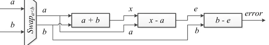
Figure 5.1 shows the adder network for hardware implementation of the Fast2Sum
algorithm using standard double precision adders for extracting the error during
addition. Here, the order of operations requires the comparison between the absolute
values of input operands a and b. If |a| < |b| then we swap these values and supply
them to the adder network. This comparison is in effect the comparison between
the exponents of operands and during addition, the operand with smaller exponent
is shifted. The adder network consists of three double precision adders and output