e- ISSN: 2278-067X, p-ISSN: 2278-800X, www.ijerd.com
Volume 15, Issue 2 (February 2019), PP.65-69
Efficient Energy for Low Power VLSI Design
V. Venkateswara Reddy
1, T.V.Pitchi Reddy
21,2Department Electronics and Communication Engineering Corresponding Author: V. Venkateswara Reddy
ABSTRACT: Recent advances in CMOS VLSI design reduce device size and due to this, the minimization of energy dissipation has become a primary critical concern. In order to design portable systems, we introduce an idea for low power and high speed switching that is adiabatic strategy which minimizes the power consumption by regaining energy drawn from the supply clock. In this paper, all work is done using SPICE tool to simulate results of the proposed technology and other strategies also; these results show empirical comparison between different parameters such as logic style, power dissipation and delay. A minimum dissipation of the energy at a certain frequency is observed i.e. an optimum frequency exists in adiabatic logic where energy consumed per cycle is minimized. These improvements show that proposed method can considerably reduce the power consumption in new design when compared to the conventional CMOS design techniques.
Keywords: Adiabatic logic, efficient charge recovery, Low power, Power clock INTRODUCTION:
--- --- Date of Submission: 10-07-2019 Date of acceptance: 28-07-2019 --- ---
I.
INTRODUCTION
Demand for low power and high speed digital circuits has motivated VLSI designers to explore new approaches in the field of designing VLSI circuits. Also, the thermal stress caused by power dissipation as heat, on chip is a major reliability issue. Therefore, reduction of power dissipation is also desirable for reliable enhancement. Energy recovery (adiabatic) logic is a promising approach, which has been originally developed for low power digital circuits . Systems having switching activities, dynamic power is a dominant factor in energy dissipation. In conventional CMOS circuits, energy dissipation can be minimized through adiabatic technique and some of energy stored in load capacitance can be reus ed instead of dissipated as heat .
The term “Adiabatic” was firstly coined at the Second Workshop on Physics and Computation in this context appears to be in 1992. Although researcher has made an earlier suggestion about energy recovery where in relation to the energy used to perform computation, “This energy could in principle be saved and reused”. There are some classical methods to reduce the dynamic power dissipation such as decreasing voltage power supply, reducing physical capacitance and reducing switching activity. Generally power supplies of adiabatic logic circuits have used constant current source to get this, while non-adiabatic circuits that have used fixed-voltage power supply.
FOUR MAIN COMPONENTS OF TOTAL POWER DISSIPATION Total power dissipation of a CMOS Circuit is given by
i) Dynamic (switching) power dissipation: P is the dynamic switching power which dissipates when Pdynamic
charging or discharging of the parasitic capacitances occurs during a node voltage transition.
ii) Leakage power dissipation: Pleakage is a combination of MOSFET switches and gate leakage power caused by carrier tunneling through thin gate oxides.
iii) Short-circuit power dissipation: Pshort circuit is the transitory power dissipation during an input signal transition when both the pull-up and pull-down network of CMOS gate are simultaneously on.
DYNAMIC POWER DISSIPATION
Figure 1. General CMOS circuit [2] Figure 2. Equivalent circuit for adiabatic switching [2] General CMOS circuit having NMOS network, PMOS network and total output load capacitance is shown in Fig. 1 [2]. The average dynamic power dissipation for this network is given as: Vi the node voltage, VDD the full voltage swing, Ci is the parasitic capacitance linked with each node in the circuit ( including the output node),represents the corresponding node transition factor associated with that node.
# of nodes
P C V V f
avg Tii i DD CLK and Ti T Switching probability, i 1 Where,
ADIABATIC LOGIC
In conventional CMOS logic circuits with rail to rail output voltage swing, each switching event causes
an energy transfer from the power supply to the output node. Depending on the input signal, in steady state either PMOS device or NMOS device is on, the remainder is off. If an input signal transition from 1 to 0 occurs, energy is drawn from the power supply at a constant voltage to charge the output capacitor to the voltage VDD. A charge of Q = CloadVDD is taken from the voltage source, an energy qua ntum of Esupply = QVDD = CloadV2DD is drawn from the power supply during this transition. The difference between the delivered energy and the stored energy is dissipated in the PMOS network. If an input signal switches from 0 to 1, in steady state, NMOS is on and PMOS is off. Charge stored on output capacitance is then dissipated via the NMOS network to ground.
To reduce the power dissipation we can minimize switching activities or load capacitance or voltage swing or apply a combination of these three. For making energy efficient logic circuits, the concept of adiabatic logic can be introduced for energy recovery.
Adiabatic Switching
Figure 3(a). Conventional CMOS logic gate [2] adiabatic logic gate Figure 3(b). The topology of an implementing the same function.
DIFFERENT LOGIC FAMILIES
Practical adiabatic families can be classified as either partially adiabatic or fully adiabatic. In a partially adiabatic logic circuit, some charge is allowed to be transferred to the ground. In a Fully Adiabatic, all the charge on the load capacitance is recovered by the power supply. Fully adiabatic circuits face problems with respect to operating speed and input power clock synchronization. Complete recovery of the power-clock is not possible through the PMOS device, so it is still only a quasi-adiabatic logic style. Many researchers have proposed techniques, methods or models for energy efficient CMOS digital circuits. We found the following, are the noteworthy contributions in the field of proposed work.
Efficient Charge Recovery Logic (ECRL)
Fig. 6(a) shows the schematic of the Efficient Charge Recovery Logic (ECRL) . Full output voltage swing is obtained because of the cross-coupled PMOS transistors in both, pre-charge and recover phases. But due to the threshold voltage of the PMOS transistors, circuit suffers from the non-adiabatic loss in both, pre-charge and recover phases.
2N-2N2P Adiabatic Logic
Figure 7(a). Basic Structures of the Adiabatic Figure 7(b). Simulated waveforms of 2N-2N2P Logic
2N-2N2P Logic
This was proposed as a modification to ECRL logic, in order to reduce the coupling effects. Fig. 7(a) shows the general schematic of the 2N-2N2P logic.
The 2N-2N2P logic uses a cross-coupled latch of two PMOSFETs and two NMOSFETs. The primary
advantage of 2N-2N2P over ECRL is that the cross- coupled NMOSFETS switches result in non-floating outputs for large part of the recovery phase. It can be seen that at the non-adiabatic loss is dependent on the load capacitance.
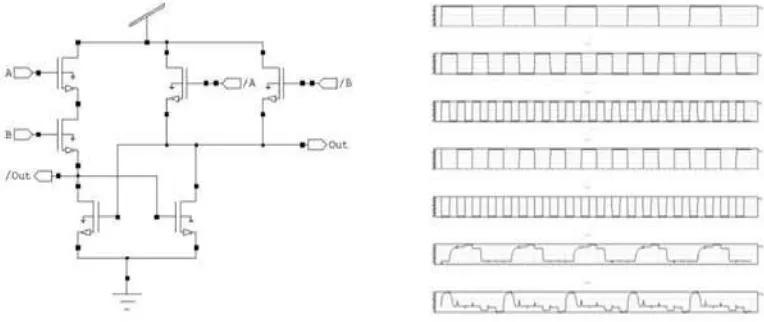
Proposed logic
In CMOS circuits, active power dissipation depends on voltage swing, node capacitances and the switching activity of the circuit (number of transitions occurred per second) which depends on the frequency of operation. Fig. 8(a) shows the general schematic of the proposed logic. Proposed research work is based on circuit level approach to minimize power dissipation in MOS circuit, in which energy loss is reduced by limiting voltage differences across conducting devices. We ensure that the voltage drop across the transistor is relatively small at the time when the switching occurs. This is accomplished by using time varying voltage waveforms. A minimum dissipation of the energy at 500 MHz clock frequency is observed. Therefore an optimum frequency exists in adiabatic logic, where energy consumed per cycle is minimum.
II.
RESULT AND DISCUSSION
The proposed logic circuit is designed based on 180 nm technology and is simulated using SPICE tool. Power clock supply is 1.8V. Evaluation of the performance of proposed logic in terms of power consumption and delay is given in table 1. ECRL and 2N-2N2P logic based NAND gates are also designed and simulated for comparison. Power consumed and delay by three technologies at operating frequency 500MHz are shown in Fig. 9(a) and 9(b) respectively.
TABLE 1: POWER AND DELAY OF TECHNOLOGIES
Logics
Frequency 500MHz
Average power consumption Delay
Proposed 5.5e-05 3.5e-10
ECRL 1.03e-04 3.6e-10
2N-2N2P 1.3e-04 3.9e-10
Figure 9(a). Comparative analysis of Power consumption Figure 9(b). Comparative analysis for delay
III.
CONCLUSION
In this paper energy efficient NAND gate based on ECRL, 2N-2N2P and proposed logic is presented. The proposed logic exhibits considerable improvement in terms of power dissipation and delay compared to ECRL and 2N-2N2P technology.
In summary, proposed logic can provide useful building block in design of energy efficient circuits.
REFERENCES
[1]. Mehrdad Khatir, Alireza Ejlali , Amir Moradi. “ Improving the energy efficiency of reversible logic circuits by the combined use of adiabatic styles”, INTEGRATION, the VLSI journal, 44, pp. 12- 21, 2011.
[2]. Sung-Mo Kang and Yusuf Leblebici, CMOS Digital Integrated Circuits - Analysis and Design, McGraw-Hill, 3rd edition, Chapter 11, pp. 481-519, 2003.
![Fig. 1 [2]. The average dynamic power dissipation for this network is given as: Vi the node voltage, VDD the full voltage swing, Ci is the parasitic capacitance linked with each node in the circuit ( including the output node),represents the corresponding node transition factor](https://thumb-us.123doks.com/thumbv2/123dok_us/1414336.1654372/2.595.98.488.80.281/dissipation-voltage-parasitic-capacitance-including-represents-corresponding-transition.webp)
![Figure 3(a). Conventional CMOS logic gate [2] adiabatic logic gate Figure 3(b). The topology of an implementing the same function](https://thumb-us.123doks.com/thumbv2/123dok_us/1414336.1654372/3.595.113.480.465.606/figure-conventional-cmos-adiabatic-figure-topology-implementing-function.webp)