University of South Carolina
Scholar Commons
Theses and Dissertations
1-1-2013
High Quality Silicon Carbide Epitaxial Growth by
Novel Fluorosilane Gas Chemistry For Next
Generation High Power Electronics
Tawhid Rana
University of South Carolina - Columbia
Follow this and additional works at:https://scholarcommons.sc.edu/etd Part of theElectrical and Computer Engineering Commons
This Open Access Dissertation is brought to you by Scholar Commons. It has been accepted for inclusion in Theses and Dissertations by an authorized administrator of Scholar Commons. For more information, please [email protected].
Recommended Citation
H
IGH QUALITY SILICON CARBIDE EPITAXIAL GROWTH BY NOVEL FLUOROSILANE GAS CHEMISTRY FOR NEXT GENERATION HIGH POWERELECTRONICS
by
Tawhid Ahmed Rana
Bachelor of Science University of Dhaka, 2003
Master of Science University of Dhaka, 2005
Submitted in Partial Fulfillment of the Requirements
For the Degree of Doctor of Philosophy in
Electrical Engineering
College of Engineering and Computing
University of South Carolina
2013
Accepted by:
Tangali S. Sudarshan, Major Professor
Grigory Simin, Committee Member
M.V.S. Chandrashekhar, Committee Member
Anthony Reynolds, Committee Member
ii
iii
DEDICATION
iv
ACKNOWLEDGEMENTS
Completion of a PhD program is an odyssey which consists of not only joyful
moments and successes but also failures and frustrations. However, at the end, the joy of
a completion always overwhelms everything else. I will always remember Professor
Sudarshan for his friendliness, positive attitude and cheerfulness during this time.
Without his positive energy it would be impossible for me to overcoming the difficulties
and finish my PhD. I would like to say thanks to Professor Sudarshan for encouraging me
in pursuing new ideas and providing me with the necessary supports in realizing these
ideas by various tools.
Besides Professor Sudarshan, Professor M.V.S. Chandrashekhar was the person
who always stood beside me by supporting new ideas and giving his valuable
suggestions, which significantly improved the content of the PhD dissertation.
I would like to thank to my colleagues and-lab members Dr. Haizheng
Song, Amitesh Shrivastava, Iftekhar Chowdhury, Dr. Peter Muzykov, David Metts,
Biplob K. Daas, Mohammad Islam (Jewel), Sabih Omar, Kevin Daniels and Shamaita
Shetu for their technical help and sample characterizations. I would like to say thanks to
my friends and family members in USA and in Bangladesh for their support during this
time.
I thankfully acknowledge my parents for their selfless support. I am greatly
v
South Carolina is a place rich in natural beauty and wonderful people. I will
specially remember the beautiful Congaree River, which was located very near to the
USC. The main idea of my PhD topic is the result of a simple thought which was sparked
in my mind while I was observing the rocks interacting with the water stream in this
heavenly Congaree River. I will always cherish my beautiful memories in South Carolina
in my heart and I hope I can take my experiences that I gained here to the next level in
vi
ABSTRACT
High quality, thick (~100µm), low doped and low defect density SiC epitaxial
films are essential for high voltage (blocking voltage >10kV), light, compact and reliable
next generation power devices. One of the significant challenges in obtaining high quality
thick SiC epitaxial films is to restrict/eliminate the Si gas-phase nucleation or aerosol
formation during growth. The generated aerosol particles adversely influence growth by
reducing the growth rate due to precursor losses, and also affect crystal quality, since the
Si droplets are carried to the crystal growth surface. Moreover, liquid aerosol particles
adhere to the various reactor parts (parasitic deposition), and contribute to their severe
degradation during epitaxial growth. These parasitic depositions are generally loosely
bound, and can be carried to the growth surface during growth as particulates, resulting in
degradation of crystal quality by introducing defects in the growing epitaxial layers. The
aforesaid condition is specifically severe at higher precursor gas flow rates or in long
duration growth required to achieve high quality thick epitaxy since parasitic deposition
and related particulate formation are also increased at these growth conditions. At this
parasitic deposition enhanced condition, the cost of growth is also expected to increase
due to frequent replacement of degraded reactor parts. Hence, cost effective, high quality
thick epitaxy is not achievable until the particle generation in the reactor is suppressed
effectively in high temperature SiC CVD. To investigate the critical issues of parasitic
vii
performed for the first time for different conventional silane and chloro-silane gases.
Based on the study of these precursors, a novel Si precursor gas tetrafluorosilane (SiF4)
was proposed to be a superior Si precursor gas specifically suitable for high temperature
SiC CVD. Initially, SiF4 is compared to DCS without any propane addition during
growth. It was found that without propane SiF4 with only hydrogen, no Si deposition
takes place in the reactor (only etches the SiC), whereas DCS deposits severe Si on the
surface making the reactor parts unusable. The ability of SiF4 not to deposit Si in the
reactor is unique and found to be very useful to achieve high quality SiC epitaxy at high
temperatures in the cleanest possible growth environment. The chemistry of SiF4 gas
precursor is utilized to eliminate Si gas phase nucleation and Si parasitic deposition
during silicon carbide (SiC) epitaxial growth, otherwise unachievable in similar growth
conditions using conventional silane (SiH4) and dichlorosilane (SiCl2H2/DCS) precursors.
Higher Si-F bond strength (565 kJ/mol) in SiF4 prevents early gas decomposition and Si
cluster formation, essential for high temperature SiC CVD, and yet enables growth of
high quality epitaxy in an improved particulate suppressed growth condition. High
quality, thick 4H-SiC epilayers >100 um have been demonstrated using SiF4 with
excellent surface morphology, polytype uniformity, crystallinity and low defect density
needed for reliable high power devices.
viii
TABLE OF CONTENTS
DEDICATION ... iii
ACKNOWLEDGEMENTS ... iv
ABSTRACT ... vi
LIST OF TABLES ... xi
LIST OF FIGURES ... xii
LIST OF SYMBOLS ... xviii
LIST OF ABBREVIATIONS ... xix
CHAPTER 1:SILICON CARBIDE ... 1
1.1INTRODUCTION ... 1
1.2PROPERTIES OF SIC ... 7
1.3SIC CRYSTAL FUNDAMENTAL ... 11
1.4GROWTH RATES ON DIFFERENT OFF CUT ANGLES ... 17
1.5GROWTH MECHANISM ... 18
1.6ETCHING PROCESS ... 21
1.7DEFECTS ... 22
1.8FORMATION AND CONVERSION OF BPD ... 25
ix
CHAPTER 2:STUDY OF SICEPITAXIAL GROWTH USING SILANE AND DICHLOROSILANE
GASES ... 33
2.1INTRODUCTION ... 33
PARTI:ANALYTICAL MODEL ... 38
2.2DIFFUSIVITY ... 38
2.3GROWTH RATE CALCULATION ... 42
PARTII:SIMULATION AND EXPERIMENTAL STUDY ... 47
2.4INFLUENCE OF GROWTH PRESSURE ... 47
2.5EXPERIMENTAL SETUP ... 48
2.6DECOMPOSITION OF SILANE AND DCS INTO ELEMENTAL SILICON ... 50
2.7GROWTH RATE VERSUS PRESSURE ... 53
2.8VARIATION OF DOPING CONCENTRATION WITH PRESSURE ... 57
2.9VARIATION OF SURFACE MORPHOLOGY WITH GROWTH PRESSURES... 61
CHAPTER 3:SICEPITAXIAL GROWTH USING FLUORINATED SILANE (SIF4) ... 65
3.1 INTRODUCTION ... 65
3.2EXPERIMENTAL SETUP ... 73
3.3THERMO-CHEMICAL STUDY OF SIH4,SIH2CL2 AND SIF4 ... 76
3.4.STUDY OF PARASITIC DEPOSITION USING SIH4,SIH2CL2 AND SIF4 ... 81
3.5.COMPARISON OF EPITAXIAL GROWTHS USING SIH4,SIH2CL2ANDSIF4 ... 82
CHAPTER 4:SICSURFACE PREPERATION (ETCHING)BY SIF4 ... 89
4.1INTRODUCTION ... 89
4.2EXPERIMENTAL ... 96
x
CHAPTER 5:EFECT OF C/SI RATIOS ON EPILAYERS GROWN ON VARIOUS OFF-CUT
SUBSTRATES USING TETRAFLUOROSILANE GAS ... 113
5.1INTRODUCTION ... 113
5.2RESULTS AND DISCUSSION ... 119
5.3C/SI VS.SURFACE MORPHOLOGY ... 136
SUMMARY AND FUTURE PROSPECTS ... 147
REFERENCES ... 153
APPENDIX A-SILICON CARBIDE CRYSTAL PLANES AND DIRECTIONS ... 160
APPENDIX B–EPITAXIAL GRAPHENE GROWTH BY SIF4GAS ... 161
APPENDIX C–SAFETY ISSUES USING SIF4GAS ... 162
APENDIX D–DRAWING OF SPLIT TUBE ASSEMBLY ... 163
xi
LIST OF TABLES
Table 1.1 Properties of various semiconductor materials ... 7
Table 2.1 Experimental and theoretical values of the diffusivities of various gas
molecules in the silane-propane and DCS-propane CVD chemistries at STP. ... 41
Table 2.2 Comparison of analytical calculation of diffusivity, boundary layer thickness and growth rate for Silane and DCS. ... 46
Table 2.3 Dissociation bonding energies (Huheey, 1972) for various bonds related to silicon carbide growth. ... 51
Table 3.1 Comparison of epilayer quality using various precursors for (T= 1550°C, P= 300 torr, H2 flow rate = 6 slm, C/Si =~1 and growth duration = 1hr; substrate
E2(TO)/E1(TO) or 4H/3C peak ratio = ~32, substrate doping = ~1x10¹⁹-N-type and
substrate XRD FWHM = ~20 arcsec). ... 83
Table 4.1 Dissociation bonding energies of various bonds found in Si precursors ... 96
Table 4.2 Free formation energy (kcal/mol) for various SiC etching reactions calculated from JANAF thermo-chemical data [21] (kinetics.nist.gov/janaf/) ... 101
Table 5.1 Current commercial specification of 3" and 4" diameter wafers ... 118
Table 5.2 : Metric for doping ΔN = ND – (-NA) = ND + NA of epilayer using various
gases. ... 122
xii
LIST OF FIGURES
Figure 1.1 Three possible stacking sequences of silicon carbide ... 12
Figure 1.2 SiC polytypes seen from different directions. ... 13
Figure 1.3 Step structure of SiC for various off cuts of 4H-SiC (towards )... 15
Figure 1.4 3D image of a kink produced due to off cut of a substrate (Si face). ... 16
Figure 1.5 Kink shape for the off cut towards a) and b) [1100] directions. ... 17
Figure 1.6 Modeled growth efficiency (qualitative indication of growth rate) as a function of off cut angles. ... 18
Figure 1.7 a) Bottom (towards [0001] x-ray view) of formed 3c on (0001) plane shows ABC stacking sequence of 3C on (0001) plane. b) Two possible sequences (twins) of formation of cubic crystal on (0001) planes of 4H off cut samples x. inclusion shows ABC sequence and y. inclusion shows ACB sequence. ... 19
Figure 1.8 Step by step animation of a step flow growth and 3C inclusion during step flow growth. 3C growths are showing in hexagonal structure for ease of drawing. ... 20
Figure 1.9 Lateral and vertical 3C growth on a 4o off cut terrace ... 21
Figure 1.10 Step by step etching process of a SiC off cut surface. ... 22
Figure 1.11 Various common SiC crystal defects delineated after KOH etching. Micropipe is a threading screw dislocation with a larger displacement. ... 23
Figure 1.12 Wastage of SiC material due to cutting at an angle towards direction. ... 24
Figure 1.13 BPD lines intersects the surface due to the off cut angle ... 26
xiii
Figure 1.15 A simple analogy to BPD propagation and conversion... 27
Figure 1.16 BPD propagation and conversion due to the variation of their directions. ... 28
Figure 1.17 Triangular defects and inverted pyramids on 4o, 4H-SiC epitaxial growth. . 30 Figure 1.18 a) Nomarsky images of Si particles on a 4H-SiC wafer. b) Nomarsky image of the epilaery grown for the same place and magnified images of the positions corresponding the the circles (insets) after etching. AFM image is shown for a pit (#9) found in the epilayer. ... 31
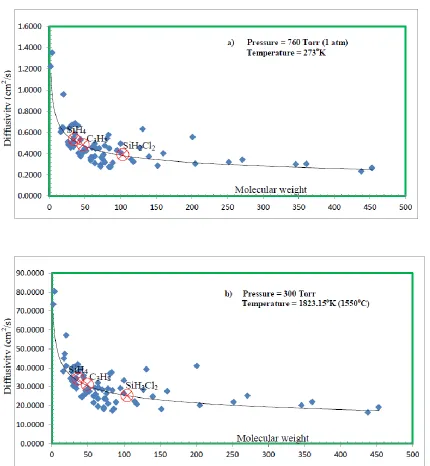
Figure 2.1 Theoretically calculated (a) diffusivity versus molecular weight plot calculated for various gases at 1 atm (760 torr) and 273oK, (b) diffusivity versus molecular weight plot for various gases at 300 torr and 1823oK (1550oC) ... 39 Figure 2.2 a) Schematic of the CVD reactor used for growth calculation. b) Boundary layer at the solid-gas interface. ... 43
Figure 2.3 Schematic diagram and boundary conditions of the CVD furnace used in simulation. The sticking coefficient for the growth surface is assumed to be 1, i.e., growth species adsorbed on the substrate surface will participate in growth. ... 49
Figure 2.4 Simulation of Si partial pressure at various growth pressures. Suppression of Si formation in DCS is clearly seen at 30 torr. Temperatures at specific locations in the reactor are shown. ... 52
Figure 2.5 Growth rate versus pressure for a) silane and b) DCS precursors: simulation and experiments ... 53
Figure 2.6 Comparison of parasitic deposition for DCS and silane in the gas injector tube shown as PQ in Figure2.1 ... 54
Figure 2.7 Doping concentration versus growth pressure. ... 59
Figure 2.8 (a) Simulated HCl partial pressure for various growth pressures for DCS. Temperatures at specific locations in the reactor are shown. (b) AFM surface roughness at various growth pressures for DCS precursor. (c) AFM images for epitaxy grown by silane precursor at various growth pressures. ... 62
xiv
Figure 3.2 (a) Reactor geometry showing the position of the split gas-injector tube (left). Split tube before growth and parasitic depositions after growth are shown for different silicon precursor gases with propane and hydrogen. The locations from where the parasitic deposition starts are marked as 1, 2 and 3 for silane, DCS and SiF4 respectively.
(b) Temperature profile in the reactor obtained using a simulation tool is shown. (c) Bar graph showing the masses of parasitic depositions on gas injector walls using silane, DCS and SiF4 precursor gases with and without propane addition. An ~80% reduction of
parasitic depositions for SiF4 with propane and a ~100% reduction without propane was
found. (T= 1550°C, P= 300 torr, H2 flow rate = 6 slm, propane flow rate = 1.6 sccm, Si
precursor flow rates = 5 sccm and duration = 1hr). ... 74
Figure 3.3Temperature versus Gibbs free energy of thermal decomposition reactions of SiH4, SiH2Cl2 and SiF4 showing very less favorable thermal decomposition reaction for
SiF4. ... 78
Figure 3.4 Particles on epilayer surface grown using various gas precursors at similar growth condition. No large particle related defects are observed for the epilayer grown using SiF4 even at higher flow rates. (T= 1550°C, P= 300 torr, H2 flow rate = 6 slm and
duration = 1hr). ... 83
Figure 3.5 AFM image of a 60um thick epilayer with excellent surface morphology grown using SiF4. ... 85
Figure 3.6 Raman analysis for epilayers grown using (a) silane, (b) DCS and (c) SiF4. A
higher E2(TO)/E1(TO) peak ratio for the epilayer grown using SiF4 (c) indicates improved
polytype uniformity compared to growths using silane (a) and DCS (b). High LOPC mode peak intensity for SiF4 grown epilayer (c) is indicative of lower dopant
incorporation compared to epilayers using silane (a) and DCS (b). ... 85
Figure 3.7 X-ray rocking curve of a epilayer grown using SiF4 gas with a FWHM of ~7.5
arcsecond... 86
Figure 3.8 Room temperature PL spectrum of a SiC epilayer grown using SiF4
demonstrates peak at 3.17eV. ... 87
Figure 4.1 Surface and subsurface damages are shown I. Initial state II. Force is applied on the diamond particle and SiC crystal is deformed, initiating surface and subsurface damages... 92
Figure 4.2. a) Electrochemical setup. b) Decoration of subsurface damages after electrochemical treatment of SiC wafers in CuSO4 solution. ... 94
Figure 4.3 Etch rates using various precursor gases with various concentrations in H2 gas
xv
Figure 4.4 Mechanism of SiC etching using TFS and H2. I. Si and C of SiC dissociate and
form Si (l) on the surface according to reactions 1 and 2 in Table 4.2, II. Si on the surface is removed by TFS (reaction 14, Table 4.2). In the absence of TFS, the removal of silicon would be by thermal evaporation (reaction 5, Table 4.2), which is much less favorable, and III. Hydrogen reacts and removes C by forming either CH4 or C3H8 gases (reactions
10 and 11, Table 4.2). ... 106
Figure 4.5 Etch rates as a function of TFS concentration in H2 gas for various off cut SiC
substrates. A trend of slightly higher etch rates were observed for higher off cut substrates. ... 109
Figure 4.6 AFM surface morphology of SiC surfaces for 0°, 4° and 8° off cut substrates etched at various TFSgas concentrations in H2. ... 110
Figure 5.1a) C/Si ratio versus doping graph for various off cut substrates using SiF4 and
C3H8 as precursor gases; b) Doping concentration versus C/Si ratio for various off cut
substrates using silane. ... 121
Figure 5.2 Comparison of C/Si ratio vs. doping for SiF4 and DCS showing the doping
change is less affected for SiF4 compared to DCS (8° off cut). ... 121
Figure 5.3 C/Si ratio distribution in the reactor (2D analysis) and distance versus C/Si ratio plot of the susceptor surface. ... 124
Figure 5.4 C/Si versus growth rate for various off cut substrates (3C growth is found above a C/Si ratio of 0.3 for on-axis substrates. ... 129
Figure 5.5 Increased 3C at the steps is shown due to the higher off cut substrates (a) compared to the lower off cut substrates (b) and considered to be the reason for lower 4H/3C for higher off cut substrates. ... 132
Figure 5.6 Raman analysis of various epilayers with different off cuts at different C/Si ratios ... 134
Figure 5.7 Bar graph showing the 4H/3C peak ratios found at various C/Si ratios for various off cut substrates. 4H/3C of the substrates (for all of cuts) are shown by dashed line... 135
Figure 5.8 AFM study of epilayers grown on 8° off cut substrates at various C/Si ratios showing no strong correlation. Roughness (r.m.s) is shown in nm. ... 136
xvi
Figure 5.10 AFM images of the epilayer sufaces (4° off cut) for varoius C/Si ratios showing variation of step bunching on the surface. 1D analysis (white line at the top of
each images) of these surfaces are shown in Figure 5.8. ... 138
Figure 5.11 1D analysis of the epilayer surface for various C/Si ratios grown on 4° off cut substrates showing the variation of macro and micro steps as a function of C/Si ratios. 140 Figure 5.12 a) Roughness measured based on the macrostep peak and troughs (calculated manually) for different C/Si ratios. b) Roughness measured based on the microstep peaks and troughs (calculated manually) for different C/Si ratios. These figures demonstrates that macrostep height is a stronger function of C/Si ratio than the microstep height. .... 141
Figure 5.13 (a) AFM images of the epitaxial growth on the vicinal on-axis surface at a C/Si ratio of 0.3. b) 1D scan analysis of the surface along [11 0]. (b) Nomarski images of the surface at different C/Si ratios. ... 143
Figure A.1 Crystal directions on the basal plane of hexagonal SiC crystal ... 160
Figure A.2 Various crystal planes of hexagonal SiC crystal ... 160
Figure B.1 Steps of the graphene growth by TFS (SiF4) gas n an inert ambient. ... 161
Figure D.1 Sketch of the injector. ... 163
Figure D.2 Sketch of injector split tube. ... 164
Figure D.3 Sketch of top plate of the gas injector. ... 165
Figure E.1 Block diagram of CVD system. ... 168
Figure E.2 CVD reactor system used for the experiments... 168
Figure E.3 Rack-1, Rack-2 and Rack-3 of the CVD system at USC ... 169
Figure E.4: CVD program by lab view ... 171
Figure E.5: MFC software (MKS controller) ... 171
Figure E.6: Profile viewer (Labview) ... 172
Figure E.7 Simplified block diagram of CVD system. ... 173
Figure E.8: pressure controller front panel. ... 174
xvii
Figure E.10: Cold Cathode Pressure unit. ... 175
Figure E.11: Gas flow meter display unit. ... 176
Figure E.12: Temperature sensor display. ... 177
xviii
LIST OF SYMBOLS
E Electric field (V/cm).
D Diffusivity (cm2/sec)
C Capacitance
V Voltage
I Current
xix
LIST OF ABBREVIATIONS
AFM ... Atomic Force Microscopy
FTIR ... Fourier Transformed Infra Red spectroscopy
SEM ... Scanning Electron Microscopy
TFS ... Tetrafluorosilane
1
CHAPTER 1
SILICON CARBIDE
In this chapter, fundamental of silicon carbide (SiC) as an electronic material and
its challenges in term of epitaxial growth will be explained. A 3D CAD model is used to
elucidate various basic crystallographic terminologies through new imageries, essential
for the understanding of silicon carbide crystal and its epitaxial growth. Growth rate
dependency is predicted for different off cuts based on these geometric models.
Conditions for homogeneous growth are explained. Various primary defects related to
SiC epitaxy is discussed in this chapter. Propagation and conversion of Basal Plane
Dislocation is discussed and it is shown that BPD aligned to the off cut direction has the
greatest chance to propagate into the epitaxial layer. Finally, some of the important
morphological defects and their origin during crystal growth are introduced in this
chapter. We believe this chapter will be a good starting point for the beginner researchers
in the field of SiC epitaxy and may also be beneficial for the experienced researcher in
the field to review their basic concepts on SiC crystal and epitaxial growth.
1.1 INTRODUCTION
There is a continuous effort in modern engineering technologies to reduce the size
of the electronic devices for the convenience of their use. Electronics used in our
2
which was available 10 years ago. Compact, light weight, cell phone, PDA and many
other pocket gadgets are using computational speed in the range of GHz frequency with
enormous amount of memories in the range of giga bytes (GBs). Most of the appliances
in our everyday life operate in low power range, usually around 100 volts and few
amperes. At this operating voltage, it is easier to make the electronics smaller since they
operate at small power and lower temperatures. Voltage domain in the regime outside of
our households is much higher, and making compact and light weight electronic devices
in that high voltage regime is extremely challenging. Heavy machineries used in the
industries operate at a much higher voltages usually in the range of kVs. The voltage used
in the national grid is much higher in the range of 10kVs to 100s of kVs. After the power
generation in a power plant, voltage in the grids stepped up much higher in the order of
100s kVs in order to reduce current induced joule heating losses during long distance
transmission. These high voltage power sources are stepped down for commercial or
household applications.
During the transmission and voltage conditioning process (e.g. step up, step
down) energy is lost. Each year about 7% of the electric energy is lost only during
transmission and distribution in US (www.eia.gov/tools/faqs/faq.cfm?id=105&t=3). The
loss of energy will be much bigger if the losses at the customer end are also included (e.g.
factories, houses, offices etc.). The picture of energy losses will be enormous and much
worrisome if the total losses in the world are considered. These energy losses not only
cost a huge amount of money every year but also affect the global climate of the world.
The USA produced about 4,106 billion kilowatt-hours of electricity in 2011.
3
(www.eia.gov/tools/faqs/faq.cfm?id=427&t=3). These fossil fuels have effect on emitting
green house gases (e.g. CO2, CH4), thus increasing the carbon footprint (Laurence A
Write, 2011) and facilitating global warming. Hence, reducing the power loss of the
electric system does not only reduce the cost but also helps to reduce environmental
pollution for a better world.
Currently, the electric grid system is built on 100 years old infrastructure where
the supply is one directional to the customer. In this system the power system (e.g. power
plant) cannot update itself to generate power based on the necessity of the consumer
usage. To make the electricity distribution and power consumption much more managed
to reduce losses and utilize them more efficiently, an intelligent grid system is required in
near future which is termed as ‘Smart Grid’. According to DOE (Department of Energy,
US), five technologies will mainly drive the Smart Grid of the future. They are
(www.energy.gov): “
Integrated communications, connecting components to open architecture for
real-time information and control, allowing every part of the grid to both “talk” and
“listen”.
Sensing and measurement technologies, to support faster and more accurate
response, such as remote monitoring, time-of-use pricing and demand-side
management
Advanced components, to apply the latest research in superconductivity, storage,
power electronics and diagnostics
Advanced control methods, to monitor essential components, enabling rapid
4
Improved interfaces and decision support, to amplify human decision making,
transforming grid operators and mangers quite literally into visionaries when it
comes seeing into their systems ”
In the smart grid system, the power supply to the clients are not one directional, rather
both the central system and the appliances can interact and find the optimal power
management for the efficient use of energy with minimum wastage. This process requires
much increased control over high voltage electric grid system at every possible node so
that they can be switched on/off or conditioned (e.g. voltage conversion etc.) more
efficiently and frequently. This is not possible with existing bulk transformer based
voltage conversion or bulky mechanical switch based switching system. To realize the
proposed smart grid system semiconductor based compact switching and power
conditioning is essential.
It can be understood easily that to realize five primary goals of Smart Grid
technology, in future, huge amount of electronic circuitry is required which will be able
to operate reliably at a much higher voltage than we use in our households, which is
beyond the handling capacity of the current silicon based technologies.
Making small, compact, light weight devices, which can operate at high voltage,
is not only highly demanded for Smart Grid systems but they are also essential for ships,
air carriers, automobiles etc. The fuel cost of the carrier is directly related to the weight of
the carrier and hence the total weight of the carrier should be as less as possible. With the
current silicon based electronics, huge, bulky cooling units are required, which increases
5
electronic materials that can be operated in the aforesaid high voltage (or power) regime,
at least theoretically, and certainly silicon carbide is the leading material of consideration.
Silicon carbide is one of the most promising new semiconductor materials for the
aforesaid applications. Silicon carbide is the choice of making high voltage, high power
electronic applications due to its outstanding properties such as high band gap, high
thermal conductivity, high breakdown electric field, low intrinsic carrier concentration
etc. (Table 1.1). Due to these properties, SiC electronic devices can be made compact,
light weight and yet operable at high voltage and high current condition. Despite these
promising properties, SiC is not yet a popular material for device fabrication due to the
difficulties to produce high quality single crystal materials. Though true exploitation of
SiCs unique properties in electronic devices should excel the performance of Si based
power devices in the current market, the primary goal of SiC material for electronic
devices is not reached yet. Further, few SiC power devices present in the market are still
much expensive than the Si based power devices. Despite reports on devices in various
literatures over 10KV (Sundaresan, Sturdevant, Marripelly, Lieser, & Singh, 2012; Zhao,
Alexandrov, & Li, 2003)and high temperature applications, commercially available
product is still in the range of 1.2 KV and at ~100 - 175°C
(www.cree.com/news-and-events/cree-news/press-releases/2013/march/2nd-gen-mosfet;
www.genesicsemi.com/index.php/news/03-05-13)only. When a product is
commercialized, the rating for the product (e.g. voltage current relation) must be strictly
maintained and it should be highly reliable for day to day operation since human lives
will be depending on these devices (e.g. uninterrupted power supply to houses, hospitals,
6
will be guaranteed over a certain period time within an acceptable tolerance limit. Silicon
carbide devices cannot ensure reliability for high voltage application until high quality
SiC materials are available. Despite high demand for high power electronics, SiC based
devices will not be sold like hot cakes for Smart Grids, ships, air carriers or automobiles
until the reliability of the devices is guaranteed by reducing the defects in the material.
Defects in electronic materials result in uncertainty in the device operation
rendering unpredictable change of the behavior of the devices over time and even
unexpected failure. In nature, ‘defects’ (in biological organisms) are well handled which
is in fact create diversity. Perhaps the term ‘defect’ does not even exist from nature’s
perspective. However, compared to the biological world in nature, human electronic
technology is still primitive. The operation of the electronic devices has to be predicted
within a ‘well defined’ regime governed by the crystal structure. It is extremely difficult
for us to predict the behavior of the electronic devices if the periodicity of the crystal (i.e.
the simplicity) is not preserved. In that consideration, for man-made electronic world, the
crystal should be ‘defect’ free so that the outcome of the devices can be well defined for
guaranteed reliability. The world we live now is based on electronic technologies. Hence
scientists constantly strive to explore new materials for electronics and improve their
crystal quality by reducing defects in them to uncover more hidden power in the nature
7
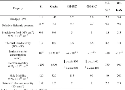
Table 1.1 Properties of various semiconductor materialsa
Property Si GaAs 4H-SiC 6H-SiC
3C-SiC
2H-
GaN
Bandgap (eV) 1.1 1.42 3.2 3.0 2.3 3.4
Relative dielectric constant 11.9 13.1 9.7 9.7 9.7 9.5
Breakdown field (MV cm-1) @ND = 1017 cm-3
0.6 0.6 3 3 1.8 2-3
Thermal Conductivity (W/cm/K)
1.5 0.5 3-5 3-5 3-5 1.3
Intrinsic carrier concentration
(cm-3)
1010 1.8 X 10⁶ ~4 x 10⁻⁸ b ~10-6 b ~10 ~10-10
Electron mobility @ND = 1016 cm-3
1200 6500
║ c-axis 800
┴ c-axis 800
║ c-axis 60
┴ c-axis 400
750 900
Hole Mobility @NA = 1016 cm-3
420 320 115 90 40 200
Saturated electron velocity (107 cms-1)
1.0 1.2 2 2 2.5 2.5
a
Adapted from (Neudeck, 2006)
b
calculated using Nc (4H) = 3.25 x 10¹⁵T3/2, Nv (4H) = 4.8 x 10¹⁵T3/2 and Nc (4H) = 3.25 x 10¹⁵T3/2, Nv (4H) = 4.8 x 10¹⁵T3/2 from the formula ni=
1.2 PROPERTIES OF SIC
Before we proceed to the discussion of the properties of SiC in comparison to
other semiconductor materials, we will discuss some basic semiconductor fundamentals
which determine the high temperature and high voltage operability of semiconductor
materials.
Considering the semiconductor is pure (no dopant), at a certain temperature, there will be
a small part of the covalent electrons liberated from the bonds due to the thermal energy
8
generated due to thermal energy are called intrinsic carriers. At room temperature,
thermal energy is 0.026eV or 26meV which is considerably lower than the bandgap of
the common electronic materials (e.g. bandgap of Si and 4H-SiC are 1.1 and 3.2
respectively). Bandgap energy of Si is 42 times higher than the thermal energy at room
temperature whereas 123 times higher than SiC bandgap energy. As a result there will be
much lower intrinsic carrier concentration present for SiC compared to Si at room
temperature. The intrinsic carrier concentration of a semiconductor material decreases
exponentially with bandgap (Pearton, 1997) by the following relation,
(1.1)
where NC is the effective density of states. For regular electronic applications, dopant
density determines the majority carrier concentration, whereas intrinsic carrier
concentration will essentially be the minority carrier concentration. An increased
minority carrier or intrinsic carrier concentration will increase the reverse bias leakage
current of the device. Hence as the temperature increases, intrinsic carrier concentration
will increase (see temperature relation in equation 1) and also the leakage current will
increase. Higher bandgap of SiC and associated lower intrinsic carrier concentration
(Table 1.1) gives SiC of its theoretical operational limit to 800°C compared to only
300°C of Si (Neudeck, 2006) .
There is another important consideration for high temperature operability which
makes SiC to be unique compared to other semiconductor material. Thermal conductivity
is the property of material to conduct heat (W/cm/K). During operation (i.e. resistive
heating due to high current flow), it is necessary to efficiently conduct the thermal energy
9
device is needed to be spread over the whole device surface and to the surrounding faster
to prevent localized damage in an integrated circuit chip. This is an extremely important
consideration for high power devices due to their high current operation and related heat
generation. A much higher thermal conductivity (~5 W/cm/K) of SiC makes it
unparalleled for high temperature operation in terms of heat management than other
common semiconductor materials.
The second consideration for high power electronics is that how much voltage can
be applied across a material without rupturing it. Maximum voltage that can be applied
across a material depends on its breakdown electric field (V/cm). When electric field is
applied across a semiconductor material, above a critical value, the material loses its
ability to withstand or resist the force created by the electric field and as a result it
raptures. As an analogy, similar phenomenon occurs during lightening spark on the sky
when electric field exceeds the breakdown electric field of the air. Higher breakdown
electric field is essential for high voltage operation of a material. Breakdown electric field
of SiC is about 10 times higher than the breakdown electric field of Si indicates that
similar thickness of SiC should block much higher voltage than Si. Breakdown voltage of
a semiconductor rectifier depends on the breakdown or critical electric (Ecrit) field as
below:
(1.2)
As a result of high breakdown field and lower intrinsic carrier concentration,
using SiC, the blocking voltage region can be made 10 times thinner and 10 times heavier
doped for Si, thus giving a 100 fold benefit in reduced resistance of the blocking region
10
Despite the aforesaid advantage of SiC for high temperature operation, mobility
of SiC is not very promising compared to GaAs, GaN or Si (Table 1.1) and hence SiC
cannot compete for high speed devices with GaAs, GaN and may not be a choice for high
frequency devices. It is to be mentioned that electron mobility of 6H SiC is isotropic
unlike that of 4H-SiC, and is much lower to the direction parallel to c-axis (Table 1.1).
Hence vertical device with SiC is not preferable and hence 4H-SiC triumphs over
6H-SiC for the choice of devices. Currently 4H-6H-SiC draws the primary interest in the
research community.
Gallium Nitride (GaN) is the strongest competitor for high voltage and high
temperature applications in the field due to its high bandgap, low intrinsic carrier
concentration, high breakdown field and higher mobility and saturated electron velocity.
However, the thermal conductivity of GaN is lower compared to SiC and GaN may not
be the best choice for high temperature devices in terms of heat management. However,
the main drawback of commercialization of GaN high power devices is considered to be
the lack of its substrates availability in the market. GaN substrates are very expensive.
Currently a six inch wafer of Si is only about $25, whereas, only a two inch GaN wafer
costs about $1900
(www.compoundsemiconductor.net/csc/indepth-details/19735741/GaN-substrates-to-challenge-silico.html) (on the other hand, for
comparison, SiC substrate will cost around few hundred dollars for a 2” wafer). To avoid
this exorbitant cost, GaN epilayers are usually grown over sapphire, SiC or Si. As a
result, interface mismatch related defects are created which increases the leakage current
11
rapidly. It is predicted that the price of GaN substrate will fall by 60% by the year 2020
(www.compoundsemiconductor.net/csc/indepth-details/19735741/GaN-substrates-to-challenge-silico.html). As GaN substrates are improved and become cheaper, it can be
assumed that that the competition between SiC and GaN to be the choice high power
electronic material will be much harder in near future unless SiC technology solves its
critical challenges meanwhile.
1.3 SIC CRYSTAL FUNDAMENTAL
1.3.1 POLYTYPES
About 200 known polytypes are found for Silicon carbide (Matsunami & Kimoto,
1997). Different polytypes have different stacking sequences. To understand the SiC
growth and related challenges it is essential to know its common polytypes in terms of
stacking sequences, crystal directions, crystal planes etc. A crystal will behave differently
from different directions. As an example, for 6H SiC, the mobility is different along
different crystal directions (Neudeck, 2006). Crystal growth is different on different
planes for growth rates, polytype replication (homogeneity) etc. To have a
comprehensive understanding of growth related issues on different crystal planes we will
first discuss about some important polytypes and their crystal structures for those
polytypes which are very widely used in SiC technologies.
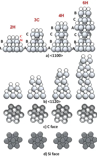
Let us discuss what polytype is. If one hexagonal close pack layer (Stack-1) is
stacked over another hexagonal closed pack layer (Stack-2) as in Figure 1.2, there are
three different possibilities they can be stacked one over another. These positions are
12
Figure 1.1 Three possible stacking sequences of silicon carbide
When SiC crystals are formed, the stacking order may take different sequences
before they repeat. Hence, SiC crystals may have different properties despite the same
atomic composition. This is called the polytypism. SiC polytypes are named based on the
number of stacks before the sequence is repeated. Various common SiC polytypes, 2H,
3C, 4H and 6H are shown using 3D modeling in Figure 1.3 These polytypes are shown
from different perspectives as if they are viewed by the audience (or seen by the gas
molecules during the growth) from different directions. The relative sizes of the atoms
are maintained in this Figure and heights of the bi-layers are kept proportional to give the
reader ‘a feel’ of viewing real SiC crystals. The polytypes stacking sequences can be seen
easily by observing Figure 1.3(a) and Figure 1.3. (b). However, for the similar polytypes,
13
Figure 1.2 SiC polytypes seen from different directions. C
14
observing the c planes (from top or bottom) in <c> direction as shown in Figure 1.3(c)
and Figure 1.3(d). Readers are advised to see various directions in the SiC crystal in the
Appendix.
Similarly, during the CVD growth, molecules ‘see’ the surface they approach the
surface from different directions. Crystal growth on a c plane (or basal plane) can take
any arbitrary polytype when gas molecules approach it as for us it is impossible to know
the polytype from the c plane only (as Fig-3c and d). So, growth on a c-plane (0001) is
highly unpredictable since it does not expose any template needed for polytype
replication during growth. Homogeneous crystal is essential for devices and this problem
can be solved by partially exposing the m planes to create a template for polytype
imitation by cutting the original crystal boule at an angle which is called the off cut angle.
Thus, to facilitate the homogeneous growth, steps are created by cutting the wafer at a
certain angle and this is called step controlled epitaxy as described in (Matsunami &
Kimoto, 1997) for silicon carbide epitaxy.
1.3.2 STEP CONTROLLED EPITAXY
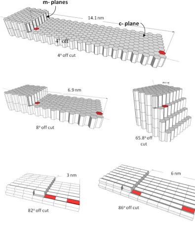
To create the template for the imitation of the polytype during the crystal growth,
it is essential to cut the crystal at an angle of usually 2°, 4°, 8°. Wafers are usually
produced by cutting at an angle towards a certain direction which is usually
for SiC. Figure 1.4 shows the step sizes for different off cut angles. Using the 3D
modeling software it was found that the step density will increase up to an off cut of 65.8
degree and reach its maximum step density for 4H-SiC. It can be inferred that the crystal
quality will be the best in term of polytype uniformity at this angle since for this off cut, a
15
Figure 1.3 Step structure of SiC for various off cuts of 4H-SiC (towards )
image of the kink, where the ideal growth should take place is shown in Figure 1.5. When
off cut is increased further, step density is reduced again, however this time, the crystal 4o off
16
plane on the surface changes. Step height is reduced and the surface of the terrace is not c
plane anymore as seen for the off cuts of 82° and 86° in Figure 1.4.
Figure 1.4 3D image of a kink produced due to off cut of a substrate (Si face).
How a kink might be different than a terrace can be apparent by observing Figure
1.5. At kinks both Si and C dangling bonds are present whereas the terrace is only
terminated either by Si or C. At the kink dangling bond from both C and Si are present
and hence kinks are energetically more favorable for homogeneous growth.
If the crystal is cut towards direction, then the kink produced at the
steps will look like Figure 1.6(a). On the other hand, if the crystal is cut towards <1100>
direction, the kink will look like Figure 1.6(b). Even though in a perfect off cut, only a
certain kind of steps Figure 1.6 (a) or (b) should exist, however, practically, the off cut is
17
mis-cut. At higher off cuts one type of step will be dominant with higher density than the
other. On the other hand, for lower off cut substrates, especially for the vicinal on axis
substrate, the density of both types of steps might be comparable in density and the
growth may take in both directions (isotropic) rendering anomaly in the step flow growth.
Figure 1.5 Kink shape for the off cut towards a) and b) [1100] directions.
1.4 GROWTH RATES ON DIFFERENT OFF CUT ANGLES
Off cut substrates have a surface with c planes and m planes (Figure 1.4). The
objective of the off cut is to provide template of the certain polytype to facilitate the
homogeneous growth as discussed earlier. The activation energy required for the growth
is very low at the kink (only 3 kcal/mol) compared to the higher activation energy
required to grow on the terrace (20 kcal/mol) (Kimoto, Nishino, Yoo, & Matsunami,
1993). Hence, kinks produced due to off cut as shown in Figure 1.5 have the highest
sticking coefficient for the growth and kinks work like a perfect sink during the growth.
Since, growth takes place (or should take place for homogenous growth) mainly at the
kinks due to very low activation energy at kinks, hence growth rate will be proportional
to the kink density on the surface. Kink density on the surface is a function of off cut
angle as shown in Figure 1.4. We used the 3D modeling tool to count the step number for
18
a certain length for various off cut angles and plot them in Figure 1.7. The y-axis in
Figure 1.7 is analogous to the step density or kink density indicating the growth
efficiency or growth rate. Step increment is not linear to the increase of off cut and does
not change for all off cut angles. The off cut angles where there is a change in step
density is shown by dots in Figure 1.7. It can be seen in Figure 1.7 that the kink density
increases rapidly until ~10° off cut almost linearly and then changes slowly at above.
There is a very little variation of step density in the range of off cut angles shown as A
and B in Figure 1.7. Step density starts decreasing again above 65.8° off cut. Though a
higher off cut will increase the growth rate, later in this chapter we will show that a
device killing defect, BPD density increases for higher off cut substrates which is
undesirable. Hence, there is a dilemma in selecting the right off cut angle for the epitaxial
growth.
Figure 1.6 Modeled growth efficiency (qualitative indication of growth rate) as a function of off cut angles.
1.5 GROWTH MECHANISM
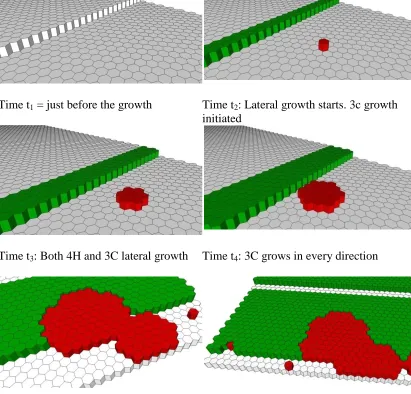
Growth on c plane (0001) is undesirable due to their tendency to form 3C
polytype since it is the plane of (111) of a cubic crystal as well (Konstantinov, Hallin,
19
Pecz, Kordina, & Janzen, 1997)with a negligible lattice mismatch. 3C nucleation on the
(0001) or c-plane and the possibility of forming 3C twins are visually depicted in Figure
1.8. As discussed earlier, the goal of cutting the substrate at a certain angle is to create the
kinks where polytype sequence is exposed for imitation by the incoming gas molecules
during the CVD process. However, c planes (terraces) on the surface as seen in Figure 1.4
are still present. Hence, the possibility of 3C formation remains during the growth. In an
ideal condition 3C growth on c plane (Figure 1.8) should be completely suppressed.
Figure 1.7 a) Bottom (towards [0001] x-ray view) of formed 3c on (0001) plane shows ABC stacking sequence of 3C on (0001) plane. b) Two possible sequences (twins) of formation of cubic crystal on (0001) planes of 4H off cut samples x. inclusion shows ABC sequence and y. inclusion shows ACB sequence.
The quality of epitaxy in terms of morphological defects (often 3C inclusion
related defects) for a given condition will depend on the terrace length. At lower off cut,
terrace or c-plane (0001) as seen in Figure 1.4 are longer. When 3C is nucleated on these
longer terraces (0001), 3C growth on the terrace will have an interaction to the step flow
growth by creating obstruction. This is illustrated in Figure 1.9 which is self explanatory.
x
y
Terrace
20
Time t1 = just before the growth Time t2: Lateral growth starts. 3c growth
initiated
Time t3: Both 4H and 3C lateral growth Time t4: 3C grows in every direction
Time t5: Initiation of other 3C Time t6: 3C growth expands and included
21
Only lateral growth of 3C polytypes was shown in Figure 9. However c plane is also
possible for vertical growth (towards [c]) for 3C growth (Figure 10), which will make the
step flow growth process more complicated.
Figure 1.9 Lateral and vertical 3C growth on a 4o off cut terrace
1.6 ETCHING PROCESS
Etching is an essential part of the SiC epitaxial growth. An ideal etching condition
will preserve the surface and should also be step mediated, taking place at the kinks.
Unlike the growth towards (if cut in this direction), the step flow during etching
is towards [1120] direction. Similar like the growth, kinks has the higher reactivity for the
etchant gas molecules since at the kink a complex arrangement of dangling bonds are
present which are more reactive (please see Figure 1.5 for a better understanding of the
atomic arrangement at the kink compared to the terrace). Hence the etching occurs more
favorably at the kink and with a lateral movement than vertical. As an example, the ideal
etching of the surface (shown in Fig-10) is elaborated step by step in Figure 1.11. Growth
22
Time t1: Initial condition Time t2: The topmost cell is removed
first since it has highest number of m-planes exposed for reaction.
Time t3: Lateral etching continues and the
step edges moves towards [1120] direction
Time t4: Any perturbation, scratch
marks etc. will be flatten
Figure 1.10 Step by step etching process of a SiC off cut surface.
From the previous discussion of growth and etching described by Figure 1.9 and Figure
1.11, we deduce the ideal conditions for homogeneous, step flow growth as following.
1. Step flow growth cannot be obstructed by any 3C nucleation or particle
obstruction.
2. Absolutely no growth on c planes or terraces is ideal.
3. Etching should be optimized to such a point that 3C nucleation is completely
etched away but the growth at the kink is preserved.
1.7 DEFECTS
There are three main dislocation widely discussed in SiC epitaxy. They are,
23
plane dislocations (BPD). The discussion these dislocations are commonly found in many
elementary books related to crystal defects (Johannes & Julia R., 1964; W. T. Read,
1953). These common defects are shown after KOH etching in Figure 1.12. Circular, or
oval shapes are indicative of their directions in the crystal related to off cut.
Figure 1.11 Various common SiC crystal defects delineated after KOH etching. Micropipe is a threading screw dislocation with a larger displacement.
Different crystal dislocations have different direction in the crystal. Dislocations are
the results of stress stored in the crystal due to deformation. The stress has a line along
which it exerts displacement force in the crystal resulting in the dislocation. When the
stress line is perpendicular to the dislocation line, then the dislocation is called screw
dislocation. On the other hand when the stress line is along with the dislocation line then
it is called an edge dislocation. On the other hand, any dislocation which lies in the basal
24
As epilayer is grown on substrate, it has the tendency to replicate the structure of the
bulk which includes crystal imperfections as well. So, defect sites in the bulk are the
primary sources of defects in the epilayer. Both screw and threading edge dislocations
propagate perfectly to the epilayer from substrate, though basal plane dislocation mostly
converts into threading edge dislocation (Ha et al., 2002; Ohno et al., 2004). Lower
elastic energy of threading edge dislocation per unit area along the growth thickness is
more preferable to form during the growth than forming the basal plane dislocation of
higher elastic energy (Ha et al., 2002). That is why it is assumed that most of the BPDs
convert in TED during epitaxial growth.
Figure 1.12 Wastage of SiC material due to cutting at an angle towards direction.
Epilayer grown on on-axis substrate is prone to nucleation of different polytypes.
As discussed earlier, this problem was solved by introducing step controlled epitaxial
growth (Matsunami & Kimoto, 1997). It is easily understood from Figure 1.13 that higher
the off cut angle, higher the amount of material will be wasted due to the cut. This is
undesirable from manufacturers’ point of view since it will increase the cost of the
material. Lower off cut angle as much as 2o off cut is often preferred by the manufacturer to keep the price low.
Bulk
Bulk
8o off cut sample
BPD line [0001]
A
B
8o
25 1.8 FORMATION AND CONVERSION OF BPD
BPD is a device killing defect in epitaxial growth which is found to propagate in
higher number from substrate to the epilayer for higher off cut angle. It was found that
for off axis samples, few of the BPDs are able to propagate through the epilayer and
emerge on the surface and the rest of them convert into TED. A to B ratio in Figure1.13
plays an important role to determine how the BPDs will propagate into the surface of
epilayer. For a lower A to B ratio (lower off cut angle) it is energetically more favorable
for BPDs to convert into TEDs (Ha et al., 2002). To the contrary, for a higher A to B
ratio (or higher off cut angle) more BPDs can propagate into the surface. So, lower off
cut angle is preferable over higher off cut angle in many ways. However higher density of
some other defects as like as triangular defect, inverted pyramid and step bunching are
observed on the epilayer grown on lower off cut angle substrate. So, there might be two
ways to eliminate BPD in SiC epitaxial growth. One might be to move to lower off cut
angle by solving its related defects; this will solve both material wastage and BPD issues.
The other solution might be to find an effective method to convert all the BPDs to TEDs
during the epitaxial growth on higher off cut substrate. However material wastage cannot
be prevented by the second.
The dislocation lines of BPDs lie on the (0001) plane. For homoepitaxial growth,
the wafer is often cut into 4o or 8o off cut angle towards direction. Due to this off cut, BPD lines intersect and emerge on the surface of the wafer (Figure 1.14). BPDs are
26 8o
<0001>
Off cut plane BPD lines
BPD lines intersects
Figure 1.13 BPD lines intersects the surface due to the off cut angle
In SiC PiN diodes, a BPD is split into two under the stress due to the current flow
and Shockley type stacking faults (SSF) are generated at basal point dislocation sites in
forward bias which greatly impairs the device performance. Most of the BPDs (70% to
90%) convert into threading edge dislocations (BPD) during epilayer growth. This can be
explained by Klapper and Küpper theory (Zhang & Sudarshan, 2005). The elastic energy
per unit growth length for the defects propagating into the epilayer is given by
W
E
cos
Fig-13: Defect propa-
gation and growth direction.
Figure 1.14 Propagation and conversion of Basal Plane Dislocation (Zhang & Sudarshan, 2005)
Energetically it is more favorable for BPDs to propagate as a TED along with the
epilayer growth direction (E direction in Figure 1.15). So, for 8o off cut substrates 70% to 90% of the BPDs convert to TEDs following this energetically easier direction.
WBPD
Direction of BPD
27 Solid A
B
N
e
e
d
le
-1
Needle-2
Needle-3
C
Figure 1.15 A simple analogy to BPD propagation and conversion.
The above is illustrated by a simple example shown in Figure 1.16. It is easily understood
that it will be the easiest to pierce the solid by needle-1 towards direction A whereas it
will be the hardest to penetrate it by needle-3 in direction C. Difficulty to pierce the
material by needle-2 will be intermediate. They are equivalent to BPD direction in 90o off cut, 0o off cut (or on axis) and 8o off cut respectively. However for a perfect on axis (0o off cut) the issue of conversion or propagation is irrelevant since no BPD line intersects
the surface in this case.
Until now, in this discussion, the direction of a BPD was considered in
one-dimensional perspective for simplicity but in reality their direction varies on a two
dimensional plane (Figure 1.17).
If we consider the real scenario in epitaxial growth in the light of above example, then
1. Highest number of BPDs should propagate into the surface for 90o off cut substrate (needle-1).
28
3. Most of the BPDs should convert into TEDs for 8o off cut (needle-2) however some BPDs will just be able to propagate. Their ratio (propagation to conversion)
will depend on the off cut angle.
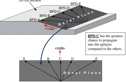
BPD-A BPD-B
BPD-C Off cut surface
<1120>
<1120>
A B C D E
B a s a l
P l a n e
B a s a l P l a n e
BPD-D
BPD-E
Figure 1.16 BPD propagation and conversion due to the variation of their directions.
Now, let us analyze Fig 17. A basal plane has been shown on the off cut substrate.
BPD directions lying on the basal planes can be different. Five BPD lines have been
shown in this Figure in different directions. It can be easily understood that BPD-C has
the highest chance to propagate as it is over the rest due to the shortest distance it needs
to travel across the epilayer. So, it can be inferred that the BPDs having the direction
most closely aligned to the direction will have greater chance to propagate
into the epilayer without any conversion (fig-16). It was found from different BPD-C has the greatest chance to propagate into the epilayer
29
experiments that around 20 to 30 percent of the BPDs propagate into the epilayer during
the growth on 8o off cut substrates. The rest convert into TEDs.
1.9 MORPHOLOGICAL DEFECTS
Morphological defects in the epilayers are comet, triangular defects, inverted
pyramids, step bunching, pits, bumps etc. Some of these defects are shown in Figure
1.18. Lower off cut angle is desirable to prevent material wastage, however lower off cut
angle generates some additional morphological defects during the epilayer growth.
Triangular defect and inverted pyramids are observed in much higher number for lower
off cut substrates. Many of the morphological defects are generated from the particulates
hampering the step flow during growth.
Effect of particulates on the epilayer growth is investigated by introducing silicon
particles artificially on the substrate before growth (Rana, Song, Chandrashekhar, &
Sudarshan, 2012a). The sizes of the particles or cluster of particles showed in Figure
1.19a vary from ~1µm to 10µm. Epitaxial films are grown with ~3-4µm thickness on this
substrate. After the growth, pits/bumps, stacking faults, screw dislocations were observed
at the corresponding locations where particles were present (Figure 1.19a and Figure
30
Figure 1.17 Triangular defects and inverted pyramids on 4o, 4H-SiC epitaxial growth.
During this particle experiment, it was found that new crystal and morphological defects
are generated due to the intentionally introduced particles with different shapes and sizes.
The density of newly generated defects in the epi will depend on the particle density in
the substrate. Even though these defects were generated due to artificially introduced
particles, a similar condition can also exist for regular epi growth. Firstly, due to the
particles introduced by the exfoliation of the parasitic deposition (i.e. deposition taking
31
Figure 1.18 a) Nomarsky images of Si particles on a 4H-SiC wafer. b) Nomarsky image of the epilaery grown for the same place and magnified images of the positions
corresponding the the circles (insets) after etching. AFM image is shown for a pit (#9) found in the epilayer.
flow. Secondly, particles may also be generated by the formation of clusters in the gas
phase due to supersaturation (especially severe at high growth rate, i.e. high precursor
concentration). These in-grown particles can also generate new defects during epi
growth similar to the artificially introduced particles discussed earlier.
In summary, various important aspects of SiC epitaxial growth are explained in
this chapter with new visual representations. This chapter will be a good supplementary
reading to understand SiC fundamentals in conjunction to various literatures, e.g.
(Matsunami & Kimoto, 1997; Neudeck, 2006). In this chapter we discussed important
terms for SiC growth which will be frequently used in the later chapters. In next chapters
we will present the results and discussion of actual epitaxial growth process using
1
2
4
5
6
7
8 9
10
a)
b)
3
32
chemical vapor deposition (CVD) process in order to solve some of the important
33
CHAPTER 2
STUDY OF SiC EPITAXIAL GROWTH USING SILANE AND
DICHLOROSILANE GASES
2.1 INTRODUCTION
Homoepitaxial growth of SiC is one of the most important processes in the
fabrication of SiC devices. Although various methods such as molecular-beam epitaxy,
liquid phase epitaxy, sublimation epitaxy and vapor-liquid-solid method are attempted in
SiC epitaxial growth, chemical vapor deposition (CVD) is still the leading and the most
attractive technique to grow thick and high quality epitaxial SiC layers (Henry, Hassan,
Bergman, Hallin, & Janzen, 2006; Palisaitis & Vasiliauskas, 2008). [25] With
development of the SiC-CVD technique, modeling and simulation become important for
reactor design, growth optimization, prediction, and better understanding of the growth
process, particularly to achieve high growth rate, high quality thick epi for electrical
power applications (Danielsson, Henry, & Janzen, 2002; Iftekher, M.V.S.Chandrasekhar,
Klein, Caldwell, & Sudarshan, 2011; Nishizawa & Pons, 2006). To understand the
benefits of growth using halogenated silanes, it is essential to understand growths using
both silane and chlorosilane chemistries. The theoretical and experimental knowledge
gain from the comparative study between silane and dichlorosilane mediated growths
presented in this chapter will lay the foundation of the next chapters where fluorinated
34
The conventional SiC-CVD process uses silane as the Si-precursor, light
hydrocarbons e.g. propane (C3H8) or ethylene (C2H4) as the C-precursor, and hydrogen as
the carrier gas. In recent years, chloride precursors such as SiCl4 and/or HCl addition are
induced to achieve high growth rate and to reduce Si-droplet formation in 4H and 6H
SiC-CVD process (F. La, Galvagno, Roccaforte, et al., 2006; Pedersen, 2008; Pedersen et
al., 2007; Wang & Ma, 2007). Numerical simulations have been carried out for
traditional precursors (Danielsson et al., 2002; Nishizawa & Pons, 2006) and some
chloride precursors (A Veneroni & Masi, 2006; Wang & Ma, 2008)for growth rate
prediction.
An accurate growth rate calculation or model prediction is not possible without
precise calculation of precursor losses due to gas phase nucleation and parasitic
deposition. Calculation of gas phase nucleation requires prediction of the number of
molecular collisions, the nucleated particle size estimation and their dynamics, which are
very complex and different for different chemistries, and under different growth
conditions with the variability of reactor geometry etc. A complete modeling tool, which
considers all of the aforesaid issues to predict the growth rate correctly for various
chemistries and growth conditions, does not currently exist. Nevertheless, despite the
limitations, simulation is still a very important tool to understand the CVD growth
process, to design experiments and to optimize growth conditions. On the other hand,
simulation can also be improved and supplemented by analyzing experimental data,
comparing them with the simulation results and optimizing the simulation for accurate