Low Power Full Adder Circuit Implemented
In Different Logic
Debika Chaudhuri
1, Atanu Nag
2, Sukanta Bose
3Assistant Professor, Modern Institute of Engineering & Technology, Bandel, Hooghly, West Bengal, India 1,2
CEGESS, BESU, Shibpur, West Bengal, India 3
ABSTRACT: The aim of this paper is to evaluate the performance of One-bit full adder cell. Different Full Adder cell with conventional static CMOS Adder is being compared. Each Cell showed different power consumption and Delay. Power consumption and speed are two important but conflicting design aspects; hence a better way to evaluate circuit performance is power delay product (PDP).The driving capability of a full adder is very important, because, full adders are mostly used in cascade configuration, where the output of one provides the input for other. Here, we have given a brief description of the evolution of full adder circuits in terms of lesser power consumption, higher speed and lesser chip size. Starting from the most conventional 28 transistor full adder we have gradually studied full adders consisting of as less as 14 transistors (14 T), 16 transistors (16T), CMOS Transmission Gate (TG), Complementary Pass-transistor Logic (CPL), Gate Diffusion Input (GDI) and Static Energy Recovery Full Adder (SERF) to meet the requirements.
KEYWORDS:CMOS Transmission Gate (TG), Complementary Pass-transistor Logic (CPL), Gate Diffusion Input (GDI), Static Energy Recovery Full Adder (SERF), 16T, 14T, Power, Delay.
I. INTRODUCTION
Designing low-power VLSI systems is significant because of the fast growing technology in mobile computation and communication. Full adders are fundamental cell in various circuits which is used for performing arithmetic operations such as addition, subtraction, multiplication, address calculation and MAC unit etc. Enhancing the performance of the full adders can significantly affect the performance of the whole system so it required to design a 1-bit Hybrid Full Adder cell which has higher speed, less power consumption and higher performance and reliability. The most effective way to reduce power consumption is the reduction of the threshold voltage in deep-sub micrometer technology and scale down the supply voltages. The design criterion of a full adder cell involves transistor counts which largely affects the design complexity of many function units such as multiplier and algorithmic logic unit (ALU). The speed of the design is limited by size of the transistors, parasitic capacitance and delay in the critical path. The driving capability of a full adder is very important as they are mostly used in cascade configuration, where the output of one provides the input for other. In the last decade, the full adder has gone through significant improvement in power consumption, speed and size, but there is no ideal full adder cell that can be used in all types of applications. In this paper, we have given a brief description of the evolution of full adder circuits in terms of lesser power consumption, higher speed and lesser chip size. We have started with the most conventional 28 transistor full adder and then gradually studied full adders consisting of as less as 14 transistors (14 T), 16 transistors (16T), CMOS Transmission Gate (TG), Complementary Pass-transistor Logic (CPL) [5], Gate Diffusion Input (GDI) [6] and Static Energy Recovery Full Adder (SERF) are proposed to meet the requirements.
II. COMPARATIVE ANALYSIS OF DIFFERENT TYPES OF FULL ADDER CIRCUITS
A. CONVENTIONAL 28T CMOS FULL ADDER:
A classical design of standard static CMOS full adder is based on regular CMOS structure with conventional pull-up and pull-down transistor providing full-swing output and good driving capabilities. The existence of the PMOS block in static CMOS circuits is a main drawback because it has low mobility compared to the NMOS. Hence, there is a need to be sized up to get desired performance. The circuit is shown in Figure 1(a).
B. TRANSMISSION GATE(TG) FULL ADDER:
Transmission gate logic circuit is a special kind of pass-transistor logic circuit. It is built by connecting a
pMOS transistor and a nMOS transistor in parallel, which are controlled by complementary control signals.
The circuit diagram is illustrated in Figure 1(b). It produces buffered outputs of proper polarity for both sum and carry.
These are inherently low power consuming with drawback of low driving capability.In the circuit we have 2 inverters
followed by two transmission gates which act as 8-T XOR. Subsequently 8-T XNOR module follows. It is a faster adder so far been reported. The circuit is simpler than the conventional adder.
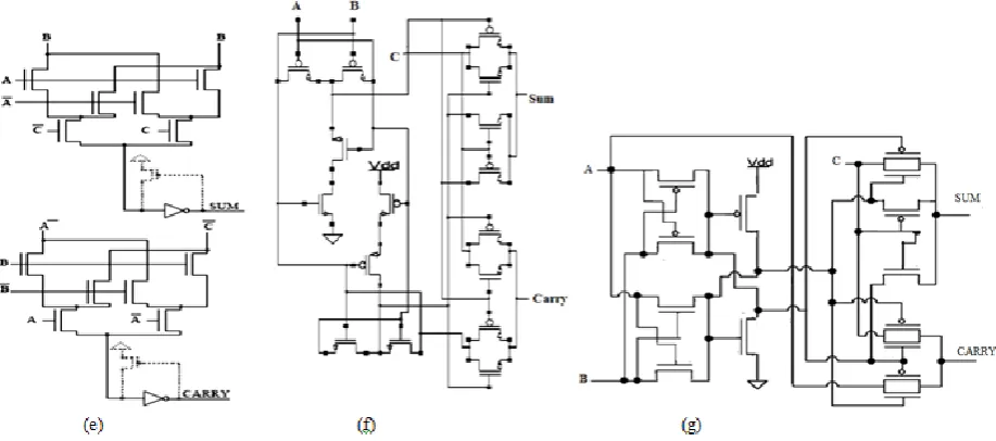
C. STATIC ENERGY RECOVERY FULL ADDER:
In this type of adder shown in Figure 1(c), the energy recovering logic reuses charge and therefore consumes less power than non-energy recovering logic. The circuit consists of two XNORs realized by 4 transistors. Sum is generated from the output of the second stage XNOR circuit. The cout can be calculated by multiplexing a and cin
controlled by (a ⊗ b). Let us consider that there is a capacitor at the output node of the first XNOR module. To
illustrate static energy recovery let us consider an example where initially a=b=0and then a changes to 1. When a and b
both equals to zero the capacitor is charged by VDD. In the next stage when breaches a high voltage level keeping a
fixed at a low voltage level, the capacitor discharges through a. Some charge is retained in a. Hence when a reaches a high voltage level we do not have to charge it fully. So the energy consumption is low here.
It should be noted that the new SERF adder has no direct path to the ground. The elimination of a path to the ground reduces power consumption. The charge stored at the load capacitance is reapplied to the control gates. The combination of not having a direct path to ground and the re-application of the load charge to the control gate makes the energy-recovering full adder an energy efficient design [12].
The circuit produces full-swing at the output nodes. But it fails to provide so for the internal nodes. As the power consumption by the circuit reduces the circuit becomes slower. Also it cannot be cascaded at low power supply due to multiple threshold problems [12].
D. FULL ADDERS REALIZED BY GATE DIFFUSION INPUT (GDI) STRUCTURES:
The circuit operation of GDI Based Full Adders shown in Figure 1(d), is exactly the same as that of previous SERF module. Sum bit is obtained from the output of the second stage of XOR circuit while Carry bit (Cout) is calculated by
multiplexing B and Cin controlled by (A XNOR B). These features give the GDI cell two extra input pins to use which
makes it flexible than usual CMOS design. It is also a genius design which is very power efficient without huge amount
of transistor count. The major problem of a GDI cell is that it requires twin-well CMOS or silicon on insulator (SOI)
process to realize. Thus, it will be more expensive to realize a GDI chip. Moreover if only standard p-well CMOS process is used, the GDI scheme will face the problem of lacking driving capability which makes it more expensive and difficult to realize as a feasible chip.
E. COMPLEMENTARY PASS-TRANSISTOR LOGIC (CPL) FULL ADDER
F.16T FULL ADDER:
1
6-T full adder is shown in Figure 1(f). The circuit consists of low power XOR and XNOR gates, pass transistors andtransmission gates. The adder offers higher speed and lower power consumption than other implementations of the full adder.
G. 14T FULL ADDER:
The 14T full adder contains a 4T PTL XOR gate, shown in Figure 1(g) , an inverter and two transmission gates based multiplexer designs for sum and Cout signals[11]. This circuit has 4 transistor XOR which in the next stage is inverted to produce XNOR. These XOR and XNOR are used simultaneously to generate sum and cout. The signals cin and cinbar are multiplexed which can controlled either by (a b) or (a ⊗ b). Similarly the cout can be calculated by
multiplexing a and cin controlled by (a b). It is a faster adder. The circuit is simpler than the conventional adder. The
power dissipation in this circuit is more than the 28T adder. However with same power consumption it performs faster [4].
(a) (b)
III. RESULT ANALYSIS
Comparative analysis between various type of Full Adder is shown in Table I showing the total no of transistor involved in the circuit, average power and delay. Figure 2 and Figure 3 depicts that power consumption and delay time both are lowest for 16T adder. The TG adder and GDI adder also have very low delay where as SERF adder has low power consumption. Figure 4 shows the variation of power delay product. From this figure it is clear that PDP is low for 16T adder and high for 14T adder.
IV. CONCLUSION
From the analysis of the above various type of Full Adder Circuits we can reach to a conclusion that the average power and Average Delay is low for 16T Full Adder. Also the PDP is low for 16T adder, so Optimization of Power (Average power) and Delay, we think that the best option is 16T Full Adder. SERF adder and TG adder are also good choice because of low PDP. Full Adders is the heart of any digital processor. Here we have shown the implementation of various type of Full Adders using MOSFET. However recent researches have shown that Carbon-Nano-Tubes have a huge potential in logic circuits. Not only will it reduce power consumption, but also increase speed substantially.
REFERENCES
[1] A. Chandrakasan, R. Brodersen, ―Low Power Design‖, Kluwer Academic Publishers, 1995.
[2] A. M. Shams, and M. A. Bayoumi, ―A Novel High Performance CMOS 1-Bit Full Adder Cell‖, IEEE Transactions on Circuit and System, vol.47, NO. 5, May, 2000.
[3] J. H. Kang and J. B. Kim, ―Design of a Low Power CVSL Full Adder Using Low-Swing Technique‖, ICSE2004 Proc. 2004, Kuala Lumpur, Malaysia.
[4] A. A. Khatibzadeh and K. Raahemifar, ―A Study and Comparison of Full Adder Cells based on the Standard Static CMOS Logic.‖, IEEE CCECE 2004 -CCGEI 2004, Niagara Falls, May 2004.
[5] S. M. Kang and Y. Leblebici, ―CMOS Digital Integrated Circuits: Analysis and Design‖, Third Edition, Tata McGraw-Hill Edition 2003, pp 307-316.
[6] A. Morgenshtein, A. Fish and A. Wagner, ―Gate-Diffusion Input(GDI): A Power-Efficient Method for Digital Combinational Circuits‖, IEEE Trans.VLSI Syst., pp. 566-581, Oct. 2002.
[7] I. Hassoune, D.Flandre, I. O’Connor and J. D. Legat, ―ULPFA: a new efficient design of a power aware full adder‖, IEEE Transactions on Circuits and Systems I-5438, 2008.
[8] R. Zimmermann and W. Fichter, ―Low –power logic styles: CMOS versus pass-transistor logic,‖ IEEE J. Solid-State Circuits, Vol. 32, July 1997,pp.1079-90
[11] J. Wang, S. Fang, and W. Feng, ―New efficient designs for XOR and XNOR functions on the transistor level‖, IEEE J. Solid-State Circuits, vol. 29, no. 7,Jul. 1994, pp. 780–786.
[12] R. Shalem, E. John, and L. K. John, ―A Novel Low Power Energy Recovery Full Adder Cell‖ in Proc. IEEE Great Lakes VLSI Symp., pp. 380– 383, Feb.1999.
[13] H. T. Bui, A. K. Al-Sheraidah and Y. Wang, ―Design and Analysis of 10-transistor Full Adders using Novel XOR-XNOR Gates‖ , Proceedings of ICSP2000.
[14] P. M. Lee, C. H. Hsu, and Y. H. Hung, ―Novel 10-T full adders realized by GDI structure‖ IEEE International Symposium on Integrated Circuits (ISIC-2007).
[15] J. F. Lin, Y. T. Hwang, M. H. Sheu and C. C. Ho, ―A novel High-Speed and Energy Efficient 10-Transistor Full Adder Design‖, IEEE Transactions on Circuits and System—I: Regular Papers, VOL. 54, NO. 5, May 2007.
[16] D. Radhakrishnan, ―Low-voltage low-power CMOS full adder,‖ in Proc. IEEE Circuits Devices Systems, vol. 148, FEB 2001, pp 19-24. [17] S. Goel, A. Kumar, M. A. Bayoumi, ―Design of Robust, Energy-Efficient Full Adders for Deep-Submicrometer Design Using Hybrid-CMOS Logic‖, IEEE Transactions on VLSI 2006.
BIOGRAPHY
D. Chaudhuricompleted her M. Tech degree inElectronics & Communication Engineering and is
working as the Assistant Professor in the Department of Electronics & Communication Engineering, Modern Institute of Engineering &Technology.
Dr. Atanu Nag is working as the Assistant Professor in the Department of Physics, Modern Institute of Engineering &Technology. He has published more than 25 papers in International Journals and attended many conferences.
Mr. S Bose completed his M. Tech degree inElectronics & Communication Engineering and is a