Growth Behavior of Compounds during Reactive Diffusion
in the Solid-Cu
/
Liquid-Sn System
S. Murakami
1, M. O
2and M. Kajihara
2,*1Graduate School, Tokyo Institute of Technology, Yokohama 226–8502, Japan
2Department of Materials Science and Engineering, Tokyo Institute of Technology, Yokohama 226–8502, Japan
Semi-infinite Cu/Sn diffusion couples prepared by an isothermal bonding technique were used to examine experimentally the kinetics of reactive diffusion in the solid-Cu/liquid-Sn system. Isothermal annealing of the diffusion couple was conducted in the temperature range of T = 753–793 K for various periods up to t = 144 ks (40 h). Owing to annealing, an intermetallic layer composed of ε-Cu3Sn with scallop
mor-phology and δ-Cu4Sn with rather uniform thickness is formed at the original Cu/Sn interface in the diffusion couple. The total thickness of the
intermetallic layer is proportional to a power function of the annealing time, and the exponent of the power function is close to unity at all the annealing temperatures. Such a power relationship holds also for the ε-Cu3Sn scallop and the δ-Cu4Sn layer. This means that volume diffusion
controls the growth of the ε-Cu3Sn scallop and the morphology of the Cu3Sn/Sn interface influences the rate-controlling process. In contrast,
the growth of the δ-Cu4Sn layer is governed by the interface reaction at the moving Cu4Sn/Cu interface. Adopting a mean value of 0.87 for
the exponent, we obtain a value of 129 kJ/mol for the activation enthalpy of the intermetallic growth. [doi:10.2320/matertrans.MC201712]
(Received July 14, 2017; Accepted September 19, 2017; Published October 20, 2017)
Keywords: reactive diffusion, intermetallic compounds, soldering, bulk diffusion, copper–tin system
1. Introduction
In the electronics industry, Cu-base alloys are widely used as conductor materials owing to high electrical conductivity, and various Sn-base alloys are preferentially utilized as Pb-free solders due to low melting temperatures. At the joint be-tween the Cu-base conductor and the Sn-base solder, an in-termetallic layer consisting of Cu6Sn5 and Cu3Sn is formed
during soldering and then gradually grows during energiza-tion heating at solid-state temperatures.1–11) Since such an
intermetallic layer is brittle and possesses high electrical re-sistivity, the intermetallic growth edgingly deteriorates the mechanical and electrical properties of the joint.
The reactive diffusion in the solid-Cu/liquid-Sn system was observed at a temperature of T = 553 K by Bartels et al.12) using Cu/Sn/Cu diffusion couples prepared by an
iso-thermal solidification technique. This technique was used also by Li et al.13) to observe the reactive diffusion at
tem-peratures of T = 533, 573 and 613 K. Both observations indi-cate that an intermetallic layer composed of Cu6Sn5 and
Cu3Sn is produced at the original Cu/Sn interface in the
dif-fusion couple in the early stages and Sn and Cu6Sn5 are
fi-nally depleted in the late stages.12,13) In contrast, an
immer-sion technique was used by Takaku et al.14) to observe the
reactive diffusion at temperatures of T = 523 and 573 K. According to their observation,14) an intermetallic layer
con-sisting of Cu6Sn5 and Cu3Sn is also formed at the original
Cu/Sn interface in the diffusion couple during annealing, where the thickness of the Cu3Sn layer is smaller than that
of the Cu6Sn5 layer. Furthermore, the total thickness of the
intermetallic layer is proportional to the square root of the annealing time. Such a relationship is usually called a para-bolic relationship. However, the proportionality coefficient of parabolic relationship is greater at longer annealing times than at shorter annealing times. This means that the growth of the intermetallic layer is accelerated at longer annealing
times. Nevertheless, any acceleration mechanisms for the parabolic relationship are not yet known.
The kinetics of reactive diffusion in various solid-metal/ liquid-metal systems was experimentally observed using an isothermal bonding (IB) technique in previous studies.15–19)
The IB technique is explained in detail elsewhere.20) In the
IB technique, the solid and liquid metals are separately pre-heated at the same temperature as the isothermal annealing temperature in a vacuum. After sufficiently long preheating, the solid and liquid metals are bonded with each other and then annealed immediately. Thus, unlike an immersion tech-nique, the temperatures of the solid and liquid metals are equivalent and remain constant during preheating, bonding and annealing in the IB technique. For instance, in a previ-ous study,18) the IB technique was used to observe
experi-mentally the kinetics of reactive diffusion in the solid-Fe/ liquid-Sn system. In that experiment, semi-infinite solid-Fe/ liquid-Sn diffusion couples were isothermally annealed at temperatures of T = 703–773 K. According to the observa-tion, a compound layer of FeSn2 with columnar
polycrystal-line microstructure is formed at the original Fe/Sn interface in the diffusion couple. The mean thickness of the FeSn2
layer is proportional to a power function of the annealing time. This relationship is designated a power relationship. Here, the exponent of the power function is typically equal to 0.6. Such a vale of the exponent means that the layer growth is controlled by volume diffusion and the morphol-ogy of growing FeSn2 grain affects the power relationship.
Thus, the kinetics of reactive diffusion in solid-metal/ liquid-metal systems is influenced by the microstructure of compounds. Such influence may contribute to the apparent acceleration for the parabolic relationship.
In the present study, the IB technique was used to exam-ine experimentally the kexam-inetics of reactive diffusion in the solid-Cu/liquid-Sn system. Semi-infinite diffusion couples consisting of pure Cu and Sn specimens were prepared by the IB technique and then isothermally annealed in the tem-perature range of T = 753–793 K. The microstructure of the
* Corresponding author, E-mail: [email protected]
annealed diffusion couple was observed in a metallographi-cal manner. The rate-controlling process of the compound growth was discussed on the basis of the observation. The discussion may provide information on the acceleration for the parabolic relationship.
2. Experimental
A commercial polycrystalline rod of pure Cu with diame-ter of 8 mm and purity higher than 99.9% was cut into co-lumnar specimens with length of 5 mm in a manner similar to a previous study.15) Each columnar specimen was
sepa-rately annealed in an evacuated silica capsule at a tempera-ture of 1173 K for a time of 2 h, followed by air cooling without breaking the capsule. The top and bottom flat- surfaces of the annealed columnar specimen were mechani-cally polished on # 800–4000 emery papers.
Polycrystalline columnar specimens with length of 30 mm were cut from a commercial rod of pure Sn with diameter of 6 mm and purity of 99.9%. Each columnar Sn specimen was encapsulated together with a mechanically polished Cu specimen in an evacuated silica capsule with inner diameter of 8.5 mm. The silica capsule was isothermally preheated for a time of 1.8 ks (0.5 h) in the temperature range between 753 K and 793 K. During preheating, the solid Cu specimen was separated from the Sn melt in the silica capsule. After preheating, a flat surface of the solid Cu specimen was im-mediately contacted with that of the Sn melt with diameter of 8.5 mm and length of 15 mm to prepare a columnar solid-Cu/liquid-Sn diffusion couple.20) The solid/liquid
dif-fusion couple was isothermally annealed for various times up to 144 ks (40 h) at the same temperature as preheating, followed by water quenching with breaking the capsule. The annealing temperature and time are denoted by T and t, respectively.
Emery papers of # 800–4000 were used to polish mechan-ically cross-sections of the annealed diffusion couple, and then alumina with diameters of 1 μm, 0.3 μm and 0.05 μm was utilized to finish the cross-sections. The microstructure of the cross-section was observed by differential interference contrast optical microscopy (DICOM). Concentrations of Cu and Sn in each phase on the cross-section were measured by electron probe microanalysis (EPMA) using pure Cu and Sn with purity of 99.99% as standard specimens under the fol-lowing conditions: the accelerating voltage was 20 kV; the probe current was 5 nA; the analyzing crystals for Cu-Kα and Sn-Lα were lithium fluoride (LiF) and polyethylene tere-phthalate (PET), respectively; and the chemical composition was evaluated by a standard ZAF correction technique.
3. Results and Discussion
3.1 Microstructure
Typical cross-sectional microstructure of the annealed dif-fusion couple is shown in Fig. 1. Figure 1 indicates a DICOM image of a diffusion couple with T = 773 K and t = 72 ks (20 h). In this DICOM image, the lower and upper re-gions are the Cu and Sn specimens, respectively. As can be seen, a layer composed of two phases with different con-trasts and shapes is observed between the Cu and the Sn. To
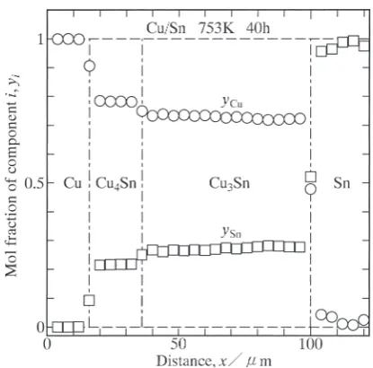
identify each phase, concentration profiles of Cu and Sn across the two-phase layer along the direction normal to the original Cu/Sn interface were measured by EPMA. A result of the EPMA measurement is indicated in Fig. 2. This figure represents the result of a diffusion couple with T = 753 K and t = 144 ks (40 h). In Fig. 2, the vertical and horizontal axes show the mol fraction yi of component i and the dis-tance x, respectively, and open circles and squares indicate the mol fractions yCu and ySn, respectively. Here, the origin
x = 0 of the distance is located in the Cu. For the EPMA measurement, however, attention was focused on phase identification of the two-phase layer. Consequently, the loca-tion of the origin is merely discreloca-tionally chosen to represent conveniently the concentration profiles. As can be seen, the phase with scallop morphology on the Sn side is ε-Cu3Sn,
and that with rather uniform thickness on the Cu side is δ-Cu4Sn. A recent phase diagram in the binary Cu–Sn
sys-tem provides that ε-Cu3Sn and δ-Cu4Sn are the stable
com-pounds at T = 753–793 K.21) Thus, all the stable compounds
Fig. 1 Cross-sectional DICOM image of the Cu/Sn diffusion couple an-nealed at T = 773 K for t = 72 ks (20 h).
[image:2.595.315.539.324.498.2] [image:2.595.322.530.547.752.2]are produced in the diffusion couple. Such microstructure was recognized in all the annealed diffusion couples. The length of the untransformed Cu specimen in the annealed diffusion couple was compared with the initial length of the corresponding Cu specimen. According to the comparison, salient parts of the ε-Cu3Sn scallop grow into the Sn, but the
two-phase layer rather totally advances towards the Cu. Hereafter, the two-phase layer is merely called the interme-tallic layer.
3.2 Growth behavior of intermetallic layer
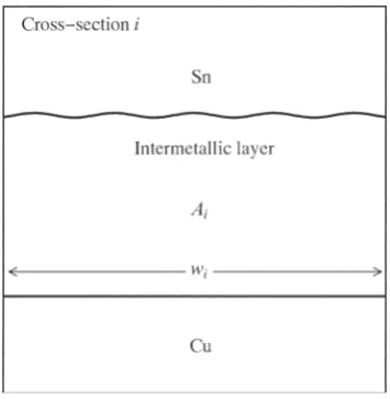
In cross-sectional DICOM images, such as that shown in Fig. 1, the intermetallic layer consisting of Cu3Sn and Cu4Sn
is distinguishable from the Cu and the Sn. Figure 3 shows schematic microstructure of the intermetallic layer on cross-section i. From the DICOM image, the area Ai of the intermetallic layer corresponding to the partial length wi of the original Cu/Sn interface in Fig. 3 was measured on each cross-section, and then the sums A and w were obtained as18)
A=
m
i=1
Ai (1a)
and
w=
m
i=1
wi (1b)
from Ai and wi, respectively, where m ≥ 5. Using the values of A and w, the total thickness l of the intermetallic layer was evaluated at each annealing time t by the following equation:18)
l= A
w. (2)
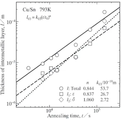
The results for T = 753, 773 and 793 K are indicated as open rhombuses, squares and circles, respectively, in Fig. 4. In this figure, the vertical and horizontal axes show the thick-ness l and the annealing time t, respectively. Here, both axes are indicated in logarithmic scales. As can be seen, the ex-perimental points are located well on a straight line at each annealing temperature. This means that l is expressed as a power function of t by the following equation.
l=k t t0
n
(3)
Here, t0 is unit time, 1 s. It is adopted to make the argument
t/t0 of the power function dimensionless. The
proportional-ity coefficient k has the same dimension as the thickness l, but the exponent n is dimensionless. As pointed out in previ-ous studies,18,19) the dimensionless argument of the power
function is essentially important; otherwise the dimension of k varies depending on the value of n. From the experimental points in Fig. 4, k and n were evaluated by the least-squares method as shown with various straight lines. The evaluated values are indicated in Fig. 4. According to the evaluation at T = 753–793 K, the overall growth rate of the intermetallic layer monotonically increases with increasing annealing temperature T.
According to Fig. 1, the interface between the Cu3Sn
scal-lop and the Cu4Sn layer is well distinguishable. From
DICOM images, such as that shown in Fig. 1, the mean thickness li of each compound was evaluated using the rela-tionships similar to eqs. (1a), (1b) and (2). Thus, there exists the following relationship among l1, l2 and l.
l=l1+l2 (4)
Here, l1 is the mean thickness of the ε-Cu3Sn scallop, and l2
is that of the δ-Cu4Sn layer. The values of l, l1 and l2 for T =
793 K are plotted against the annealing time t as open cir-cles, squares and rhombuses, respectively, in Fig. 5. In Fig. 5, like Fig. 4, the vertical and horizontal axes indicate the logarithms of li and t, respectively, and the open symbols lie well on a straight line for each compound. Therefore, we consider that li is expressed as a power function of t by the following equation of the same formula as eq. (3).
li=ki tt 0
n
(5)
From the experimental points in Fig. 5, ki and n for li in eq. (5) were evaluated by the least-squares method as shown
Fig. 3 Schematic of morphology for the intermetallic layer on cross-sec-tion i.
[image:3.595.325.530.553.752.2] [image:3.595.80.258.582.764.2]with various straight lines. The evaluated values are indi-cated in Fig. 5. Since the open squares and rhombuses are slightly scattered, the difference in the growth rate between the Cu3Sn scallop and the Cu4Sn layer cannot be
conclu-sively estimated from the result in Fig. 5.
3.3 Rate-controlling process
The mean vales of n for l, l1 and l2 are plotted as open
cir-cles with error bars in Fig. 6. As can be seen, n is greater than 0.5 and close to unity. When the layer growth is con-trolled by volume diffusion, n is equal to 0.5.22–31) Such a
re-lationship is called the parabolic rere-lationship as mentioned earlier. For precipitation of a second phase into an untrans-formed matrix in binary alloy systems, the growth of the second phase controlled by volume diffusion usually obeys the parabolic relationship. If the shape of the second phase is a paraboloid of revolution or a parabolic cylinder, however, the longitudinal growth of the second phase occurs accord-ing to the linear relationship even for the diffusion rate- controlling process.32–36) Here, the linear relationship means
that the length of the second phase linearly increases in pro-portion to the annealing time. As shown in Fig. 6, n is greater than 0.5 and rather close to unity for the ε-Cu3Sn
scallop. According to the DICOM image in Fig. 1, the Cu3Sn/Sn interface is gathered considerably. For the
precip-itation mentioned above, diffusion of solute atoms occurs in the untransformed matrix towards the second phase. On the other hand, for the migration of the Cu3Sn/Sn interface,
dif-fusion of Cu atoms takes place in the ε-Cu3Sn scallop and
the molten Sn across the Cu3Sn/Sn interface. However, the
diffusion rate is much greater in the molten Sn than in the ε-Cu3Sn scallop. Consequently, the diffusion in the molten
Sn predominates in the migration behavior of the Cu3Sn/Sn
interface and thus the growth behavior of the ε-Cu3Sn
scal-lop. Here, the molten Sn and the ε-Cu3Sn scallop correspond
to the untransformed matrix and the second phase, respec-tively, for the precipitation. The value of n close to unity in-dicates that the growth of the ε-Cu3Sn scallop is controlled
by volume diffusion and affected by the gathered morphol-ogy of the Cu3Sn/Sn interface. Influence of the interface
morphology on the value of n is extensively discussed in a previous study.18) On the other hand, unlike the Cu
3Sn/Sn
interface, the Cu4Sn/Cu3Sn and Cu/Cu4Sn interfaces are
relatively smooth as indicated in Fig. 1. Hence, the contribu-tion of the interface morphology to the value of n may be negligible for the growth of the δ-Cu4Sn layer. Nevertheless,
as shown in Fig. 6, n is close to unity also for the δ-Cu4Sn
layer. If interface reaction governs the layer growth, n is equivalent to unity.37–50) As previously mentioned, the δ-Cu4Sn layer grows mainly into the Cu. Thus, the migration
rate is greater for the Cu/Cu4Sn interface than for the
Cu4Sn/Cu3Sn interface. Consequently, the interface reaction
at the moving Cu/Cu4Sn interface controls the growth of the δ-Cu4Sn layer. Since n is close to unity for both l1 and l2, it
[image:4.595.67.272.335.535.2]becomes approximately unity also for l as indicated in Fig. 6.
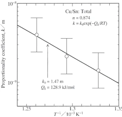
The values of n for l are plotted against the annealing tem-perature T as open circles with error bars in Fig. 7. As can be seen, n is rather insensitive to T. Considering an equivalent value of n at all the annealing temperatures, k and n were si-Fig. 5 The thicknesses l, l1 and l2 versus the annealing time t shown as
open circles, squares and rhombuses, respectively, at T = 793 K.
[image:4.595.323.528.572.770.2] [image:4.595.66.273.585.773.2]multaneously evaluated from the experimental points in Fig. 4 by the least-squares method. The evaluated value of n is shown as a solid circle with error bars in Fig. 7, and those of k are plotted against T as open circles with error bars in Fig. 8. In Fig. 8, the vertical axis indicates the logarithm of k, and the horizontal axis shows the reciprocal of T. As can be seen in Fig. 8, the open circles are located well on a straight line within experimental uncertainty, and hence the dependence of k on T is expressed by the following equation.
k=k0exp − Qk
RT (6)
Here, k0 is the pre-exponential factor, Qk is the activation en-thalpy, and R is the gas constant. The values of k0 and Qk were evaluated from the open circles by the least-squares method as shown with a solid line in Fig. 8. The evaluation provides Qk = 129 kJ/mol. This value of Qk corresponds to the activation enthalpy for the intermetallic growth con-trolled by the volume diffusion with needle-like morphology of ε-Cu3Sn and the interface reaction with layer morphology
of δ-Cu4Sn.
4. Conclusions
To examine the kinetics of reactive diffusion in the solid-Cu/liquid-Sn system, semi-infinite Cu/Sn diffusion couples were prepared by the isothermal bonding technique and then immediately annealed for various periods at tem-peratures of T = 753–793 K. At these temtem-peratures, ε-Cu3Sn
and δ-Cu4Sn are the stable intermetallic compounds in the
binary Cu–Sn system.21) During annealing, the intermetallic
layer consisting of the Cu3Sn scallop and the Cu4Sn layer is
produced at the original Cu/Sn interface in the diffusion couple. The mean thicknesses of the Cu3Sn scallop and the
Cu4Sn layer increase in proportion to a power function of
the annealing time at T = 793 K. Here, the exponent n of the power function is close to unity. Such a power relationship holds also between the total thickness of the intermetallic layer and the annealing time at T = 753–793 K. If growth of
a compound layer is governed by interface reaction, n is equal to unity. Furthermore, the value n = 1 is realized also for the growth of a needle-like compound controlled by vol-ume diffusion. Thus, the growth of the Cu3Sn scallop is
gov-erned by volume diffusion, but that of the Cu4Sn layer is
controlled by interface reaction.
Acknowledgements
The authors are grateful to Dr. Y. Tanaka at Tokyo Institute of Technology, Japan, for stimulating discussions. The present study was partially supported by a Grant-in-Aid for Scientific Research from the Ministry of Education, Culture, Sports, Science and Technology of Japan.
REFERENCES
1) L. Zakraysek: Weld. Res. Supplement (Nov.) 536 (1972) 536–541. 2) K.N. Tu: Acta Metall. 21 (1973) 347–354.
3) M. Onishi and H. Fujibuchi: Trans. JIM 16 (1975) 539–547.
4) H.N. Keller: IEEE Trans. Compon. Hybrids. Manuf. Tech. CHMT-2 (1979) 180–195.
5) H.N. Keller and J.M. Morabito: Surf. Interface Anal. 3 (1981) 16–22. 6) J.O.G. Parent, D.D.L. Chung and I.M. Bernstein: J. Mater. Sci. 23
(1988) 2564–2572.
7) A.J. Sunwoo, J.W. Morris, Jr. and G.K. Lucey, Jr.: Metall. Trans., A, Phys. Metall. Mater. Sci. 23A (1992) 1323–1332.
8) P.T. Vianco, P.F. Hlava and A.L. Kilgo: J. Electron. Mater. 23 (1994) 583–594.
9) D.R. Frear and P.T. Vianco: Metall. Trans., A, Phys. Metall. Mater. Sci. 25A (1994) 1509–1523.
10) S. Choi, T.R. Bieler, J.P. Lucas and K.N. Subramanian: J. Electron. Mater. 28 (1999) 1209–1215.
11) T. Takenaka, S. Kano, M. Kajihara, N. Kurokawa and K. Sakamoto: Mater. Sci. Eng. A 396 (2005) 115–123.
12) F. Bartels, J.W. Morris, G. Dalke and W. Gust: J. Electron. Mater. 23 (1994) 787–790.
13) J.F. Li, P.A. Agyakwa and C.M. Johnson: Acta Mater. 59 (2011) 1198–1211.
14) Y. Takaku, X.J. Liu, I. Ohnuma, R. Kainuma and K. Ishida: Mater. Trans. 45 (2004) 646–651.
15) Y. Tanaka, M. Kajihara and Y. Watanabe: Mater. Sci. Eng. A 445–446 (2007) 355–363.
16) Y. Tanaka and M. Kajihara: Mater. Trans. 50 (2009) 2212–2220. 17) Y. Tanaka and M. Kajihara: J. Mater. Sci. 45 (2010) 5676–5684. 18) M. Hida and M. Kajihara: Mater. Trans. 53 (2012) 1240–1246. 19) A. Nakane, T. Suzuki, M. O and M. Kajihara: Mater. Trans. 57 (2016)
838–845.
20) M. Kajihara and Y.Tanaka: Japanese Patent, Registration No. 5278995 (2013).
21) T.B. Massalski, H. Okamoto, P.R. Subramanian and L. Kacprzak: Binary Alloy Phase Diagrams, vol. 2 (ASM International, Materials Park, OH, 1990) p. 1482.
22) M. Kajihara: Acta Mater. 52 (2004) 1193–1200. 23) M. Kajihara: Mater. Sci. Eng. A 403 (2005) 234–240. 24) M. Kajihara: Mater. Trans. 46 (2005) 2142–2149.
25) M. Kajihara: Defect and Diffusion Forum 249 (2006) 91–96. 26) M. Kajihara: Mater. Trans. 47 (2006) 1480–1484.
27) Y. Tanaka and M. Kajihara: Mater. Trans. 47 (2006) 2480–2488. 28) M. Kajihara and T. Yamashina: J. Mater. Sci. 42 (2007) 2432–2442. 29) M. Kajihara: Mater. Trans. 49 (2008) 715–722.
30) M. Kajihara: Mater. Trans. 51 (2010) 1242–1248. 31) M. Kajihara: Mater. Trans. 53 (2012) 1896–1904. 32) A. Papapetrou: Z. Kristallogr. 92 (1935) 89–130.
33) G.P. Ivantsov: Dokl. Akad. Nauk SSSR 58 (1947) 567–569. 34) G. Horvay and J.W. Cahn: Acta Metall. 9 (1961) 695–705. 35) R. Trivedi: Acta Metall. 18 (1970) 287–296.
36) P.E.J. Rivera-Diaz-del-Castillo and H.K.D.H. Bhadeshia: Mater. Sci. Fig. 8 The proportionality coefficient k versus the annealing temperature
[image:5.595.66.269.569.763.2]Technol. 17 (2001) 25–29.
37) Y. Yamamoto and M. Kajihara: Mater. Trans. 42 (2001) 1763–1770. 38) Y. Muranishi and M. Kajihara: Mater. Sci. Eng. A 404 (2005) 33–41. 39) T. Hayase and M. Kajihara: Mater. Sci. Eng. A 433 (2006) 83–89. 40) K. Mikami and M. Kajihara: J. Mater. Sci. 42 (2007) 8178–8188. 41) Y. Yamamoto and M. Kajihara: J. Electron. Mater. 37 (2008)
1710–1720.
42) M. Kajihara and Y. Tejima: J. Phys.: Conf. Ser. 165 (2009) 012091, 1–4.
43) Y. Tejima, S. Nakamura and M. Kajihara: J. Mater. Sci. 45 (2010) 919–928.
44) M. O and M. Kajihara: Mater. Trans. 52 (2011) 677–684.
45) M. O, Y. Takamatsu and M. Kajihara: Mater. Trans. 55 (2014) 1058–1064.
46) M. Hashiba, K. Masui and M. Kajihara: Mater. Trans. 56 (2015) 30–39.
47) M. Nakayama and M. Kajihara: Mater. Trans. 56 (2015) 798–802. 48) Y. Takamatsu, M. O and M. Kajihara: Mater. Trans. 58 (2017) 16–22. 49) M. Nakayama, M. O and M. Kajihara: Mater. Trans. 58 (2017)
561–566.