Kinetics of Solid-State Reactive Diffusion between Co and Sn
Minho O
1, Yoshiki Takamatsu
1and Masanori Kajihara
2,+1Graduate School, Tokyo Institute of Technology, Yokohama 226-8502, Japan 2Department of Materials Science and Engineering, Tokyo Institute of Technology, Yokohama 226-8502, Japan
To examine growth behavior of¡-CoSn3at solid-state temperatures, kinetics of reactive diffusion between Co and Sn was experimentally observed using sandwich Sn/Co/Sn diffusion couples prepared by a diffusion bonding technique. The diffusion couples were isothermally annealed in the temperature range of 433473 K for various times up to 744 h. Owing to annealing, an intermetallic layer consisting of CoSn3 was formed at the original interface in the diffusion couple. The mean thickness of the intermetallic layer increases in proportion to a power function of the annealing time. The exponent of the power function takes values of 0.67 and 0.62 at 433453 and 473 K, respectively. These values of the exponent indicate that volume diffusion predominantly controls the layer growth and interface reaction partially contributes to the rate-controlling process. [doi:10.2320/matertrans.M2014023]
(Received January 20, 2014; Accepted April 16, 2014; Published May 30, 2014)
Keywords: cobalttin system, compound, solid-state diffusion, interconnection, under bump metallization
1. Introduction
The scaling-down of three-dimensional integration for electronic device results in decreasing bond pad pitch and smaller solder ball diameters. As an under bump metalliza-tion (UBM) material, Cu is widely used in electronics interconnection and packaging.15)Recently, the capability of
Co as a new UBM material for Sn-base solder bump has been investigated by many researchers.614)If Co is interconnected
with a Sn-base solder, CoSn compounds may be formed at the interconnection during soldering and then will gradually grow due to solid-state heating under usual energization conditions. Since such intermetallic compounds are generally brittle and possess high electrical resistivities, the compound growth deteriorates the electrical and mechanical properties of the interconnection. Thus, for application of Co, reliable information on kinetics of reactive diffusion between Co and the Sn-base solder at solid-state temperatures is essentially important.
The solid-state reactive diffusion in the Cu/Sn system was experimentally observed in a previous study.15) In this
experiment, sandwich Sn/Cu/Sn diffusion couples were prepared by a diffusion bonding technique and then isothermally annealed at temperatures of T=433473 K. At all the annealing temperatures, an intermetallic layer composed of Cu6Sn5and Cu3Sn is formed at the original Cu/
Sn interface in the diffusion couple. The total thickness of the intermetallic layer increases in proportion to a power function of the annealing time. The exponent of the power function is close to 0.5 at T=473 K but becomes 0.37 and 0.43 at T=433 and 453 K, respectively. If the growth of the intermetallic layer is controlled by volume diffusion, the exponent is equal to 0.5.16)On the other hand, the exponent becomes smaller 0.5, if boundary diffusion contributes to the rate-controlling process of the layer growth and grain growth occurs in the intermetallic layer.17) Even though the layer
growth is purely governed by boundary diffusion, however, the exponent is equivalent to 0.5 unless grain growth takes
place in the intermetallic layer.17) Thus, for the reactive diffusion in the Cu/Sn system,15) volume diffusion is the rate-controlling process atT=473 K but boundary diffusion contributes to that atT=433453 K.
In a previous study,18) the solid-state reactive diffusion in the Ni/Sn system was examined experimentally. In this experiment, like the Cu/Sn system,15) sandwich Sn/Ni/Sn
diffusion couples were prepared by a diffusion bonding technique and then isothermally annealed at temperatures of
T=433473 K. At the interface in the annealed diffusion couple, a layer of Ni3Sn4 was observed atT=453473 K,
but granular particles of Ni3Sn4 were recognized at T=
433 K. Also in this case, the Ni3Sn4layer grows according to
the power relationship. The exponent of the power function is 0.46 and 0.41 atT=453 and 473 K, respectively. Hence, the layer growth of Ni3Sn4is controlled by boundary and volume
diffusion, and grain growth occurs in Ni3Sn4. Therefore, the
rate-controlling process of reactive diffusion varies depend-ing on the annealdepend-ing temperature and the metal system. Although the layer growth of Ni3Sn4 may be accelerated by
boundary diffusion, the overall growth rate is smaller for Ni3Sn418)than for Cu6Sn5and Cu3Sn.15)
The reactive diffusion in the Co/Sn system was exper-imentally observed by Wang and Chen9) using Co/Sn
diffusion couples prepared by a soldering technique. In their experiment, pure Co specimens were soldered with pure Sn at
T=553 K and then quenched into water. After quenching, the diffusion couple was annealed at temperatures of
T=423473 K for various periods. At the original Co/Sn interface in the diffusion couple, an intermetallic layer consisting of CoSn3 is produced during soldering and then
grows during annealing. In the binary CoSn system,19) ¢ -CoSn3 is stable at T=548618 K, but ¡-CoSn3 becomes
stable atT<548 K. According to their observation,9)the¢ -CoSn3 layer with a thickness of about 0.5 µm is formed at
the original Co/Sn interface in the diffusion couple during soldering at T=553 K. Since ¢-CoSn3 transforms into ¡
-CoSn3atT<548 K, the preformation and the transformation
of ¢-CoSn3 may influence the growth of ¡-CoSn3 during
annealing atT=423473 K. To examine the growth
behav-+Corresponding author, E-mail: kajihara@materia.titech.ac.jp
ior of ¡-CoSn3 at T<548 K, this influence should be
eliminated. However, no reliable information on growth behavior of ¡-CoSn3 without the influence of ¢-CoSn3 is
available. To examine such growth behavior, the solid-state reactive diffusion in the Co/Sn system was experimentally observed at T=433473 K using a diffusion bonding technique in the present study.
2. Experimental
Polycrystalline plate specimens of pure Sn with a size of 12 mm©5 mm©2 mm were prepared by cold rolling and spark erosion from a commercial 1 kg rectangular ingot of pure Sn with purity of 99.99%. The cold-rolled plate specimens were separately annealed in evacuated silica capsules at 473 K for 2 h, followed by air cooling without breaking the capsules. The annealed Sn plate specimens were chemically polished in an etchant consisting of 20 vol% of nitric acid, 20 vol% of hydrochloric acid and 60 vol% of distilled water. The two surfaces with an area of 12 mm©5 mm of each Sn plate specimen were mechanically polished on # 800 emery paper. One of the two polished surfaces was again mechanically polished on # 10004000 emery papers until a depth of 100 µm and thenfinished using diamond with a diameter of 1 µm.
Sheet specimens with a size of 20 mm©7 mm©0.4 mm were cut from a pure Co commercial sheet with dimensions of 50 mm©50 mm©0.4 mm and purity of 99.9% and then separately annealed in evacuated silica capsules at 1173 K for 2 h, followed by air cooling without breaking the capsules. The annealed sheet specimens were chemically polished in nitrohydrochloric acid for 60 s.
After chemical polishing, a Co sheet specimen was immediately sandwiched between the finished surfaces of two freshly prepared Sn plate specimens in ethanol by the technique used in a previous study.15)The sandwiched Sn/ Co/Sn couple was fastened between two plates made of 18Cr8Ni austenitic steel with molybdenum screws; this process generated thermal compressive stress in the couple upon heating because of the lower coefficient of thermal expansion of molybdenum compared with the couple and the austenitic steel. A mica sheet with dimensions of 12©5©0.2 mm was inserted between the Sn plate and the austenitic steel to avoid diffusion bonding. The fastened couples were dried completely and then diffusion bonded by heat-treating them in an oil bath with silicone oil for 96, 28.5 and 24 h at 433, 453 and 473 K, respectively. After the heat treatment, the diffusion couples were isothermally annealed at 433, 453 and 473 K for various times up to 648, 527.1 and 410 h, respectively. The summation of the heat-treating and annealing times is hereafter merely called the annealing time
t, and the annealing temperature is denoted by T. Cross-sections of the annealed diffusion couple were mechanically polished using diamond with diameters of 15, 3 and 1 µm, and then finished with an OP-S liquid manufactured by Struers Ltd. The microstructure of the cross-section was observed by differential interference contrast optical mi-croscopy (DICOM). Concentrations of Co and Sn in each phase on the cross-section were measured by electron probe microanalysis (EPMA) using 99.99% pure Co and Sn as
standard specimens under the following conditions: the accelerating voltage was 20 kV; the probe current was 5 nA; the analyzing crystal was lithium fluoride (LiF) for CoK¡ and polyethylene terephthalate (PET) for SnL¡; and the chemical composition was evaluated using a standard ZAF correction technique.
3. Results and Discussion
3.1 Microstructure
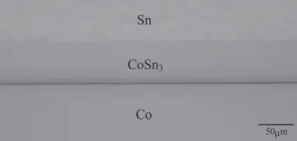
A typical cross-sectional DICOM image of the Sn/Co/Sn diffusion couple annealed at T=453 K for t=334 h (1.20 Ms) is shown in Fig. 1. In thisfigure, the bottom and top regions are the Co and Sn specimens, respectively. As can be seen, a layer with rather uniform thickness is formed at the original Co/Sn interface in the diffusion couple. To identify this layer, concentration profiles of Co and Sn were determined by EPMA along the direction normal to the original interface. A result for the diffusion couple annealed atT=473 K fort=166 h (568 ks) is indicated in Fig. 2. In this figure, the ordinate and the abscissa show the mol fraction yi of componenti and the distance x, respectively, and open squares and circles represent the mol fractionsyCo
and ySn, respectively. As can be seen, the layer is CoSn3. Fig. 1 Cross-sectional DICOM image of the Sn/Co/Sn diffusion couple
annealed atT=453 K fort=334 h (1.20 Ms).
[image:2.595.321.533.72.173.2] [image:2.595.316.536.222.435.2]According to a recent phase diagram in the binary CoSn system,19)Co3Sn2, CoSn and CoSn2as well as CoSn3exist as
stable compounds atT=433473 K. However, only CoSn3
was clearly recognized for all the annealed diffusion couples in the present study. If the interdiffusion coefficient of a compound is small at an experimental annealing temperature, the compound cannot grow to visible thicknesses within realistic annealing times.16) This implies that the
interdiffu-sion coefficient is much smaller for Co3Sn2, CoSn and CoSn2
than for CoSn3atT=433473 K. In Fig. 1, a slightly dark
thin layer with a thickness of about 6 µm may be detected on the Co side in the CoSn3layer. The detection of the slightly
dark thin layer in a DICOM image is attributed to the surface relief of CoSn3 formed by finishing with the OP-S liquid.
During annealing atT=433473 K, the CoSn3layer grows
mainly towards the Sn side and merely slightly towards the Co side.
3.2 Growth behavior of intermetallic layer
As previously mentioned, the CoSn3 layer with rather
uniform thickness is formed at the original Co/Sn interface in the diffusion couple owing to isothermal annealing at
T=433473 K. Hereafter, the CoSn3 layer is called the
intermetallic layer. The schematic morphology of the intermetallic layer on cross-section i is shown in Fig. 3. From DICOM images such as that shown in Fig. 1, the area
Ai of the intermetallic layer corresponding to the partial length wi of the original Co/Sn interface in Fig. 3 was measured on each cross-section, and then the sums Aand w were obtained as20)
A¼Xm i¼1
Ai (1a)
and
w¼Xm i¼1
wi (1b)
fromAiand wi, respectively, wherem²5. Using the values ofAandw, the mean thicknesslof the intermetallic layer was evaluated at each annealing time tby the equation20)
l¼Aw: ð2Þ
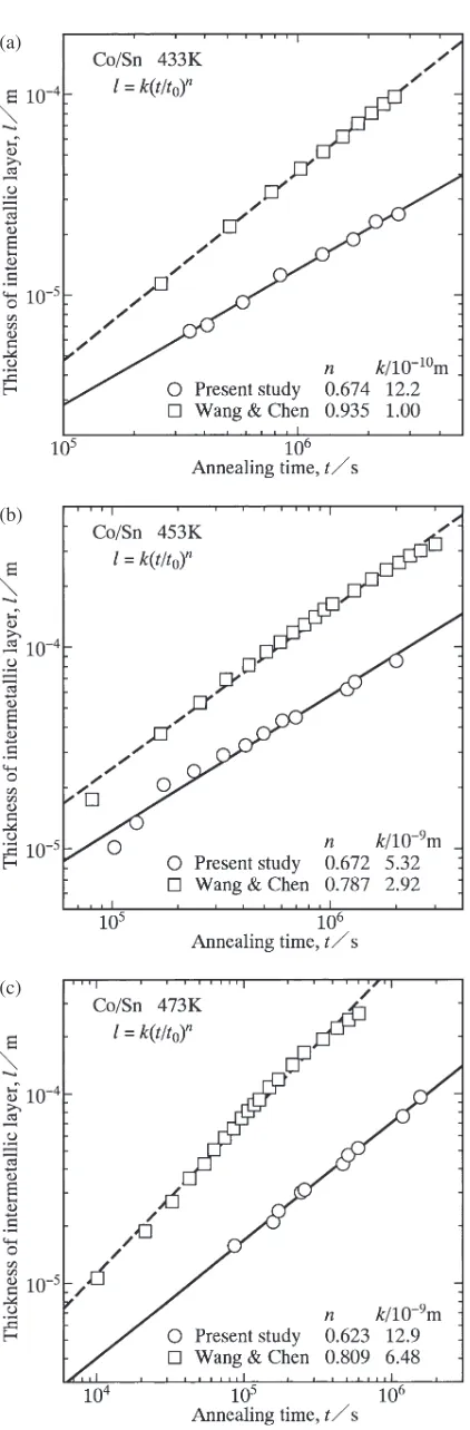
The results of T=433473 K are plotted as various open symbols in Fig. 4. In thisfigure, the ordinate and the abscissa show the logarithms oflandt, respectively. As can be seen, the thickness l increases monotonically with increasing annealing time t. Furthermore, the plotted points of each annealing temperature are located well on a straight line. Consequently, l is expressed as a power function of t as follows.
l¼k tt 0
n
ð3Þ
Here, t0 is unit time, 1 s, which is adopted to make the argument t/t0 of the power function dimensionless. The proportionality coefficientk has the same dimension as the thickness l, and the exponent n is dimensionless. From the points plotted in Fig. 4,kandnwere determined by the least-squares method as shown with various straight lines. The determined values are indicated in Fig. 4.
As mentioned in Section 1, the reactive diffusion in the Co/Sn system was experimentally observed by Wang and Chen9) using Co/Sn diffusion couples prepared by a
soldering technique. For the preparation of the Co/Sn diffusion couple in their experiment, pure Co specimens were soldered with pure Sn at 553 K and then quenched into water. After quenching, the diffusion couple was annealed at temperatures of T=423473 K for various periods. At the original Co/Sn interface in the diffusion couple, an intermetallic layer consisting of CoSn3 is produced during
soldering and then grows during annealing. Their exper-imental results ofT=433, 453 and 473 K are shown as open squares in Fig. 5(a), 5(b) and 5(c), respectively. In Fig. 5, like Fig. 4, the ordinate and the abscissa indicate the logarithms of l and t, respectively. As can be seen, the power relationship between l and t holds also for the open squares in Fig. 5. From the open squares, kand nin eq. (3)
Fig. 3 Schematic of the morphology of the intermetallic layer for cross-sectioni.
[image:3.595.318.535.67.276.2] [image:3.595.74.266.67.258.2]were determined by the least-squares method as shown with dashed lines. The determined values are indicated in Fig. 5. On the other hand, the results ofT=433, 453 and 473 K in
Fig. 4 are represented as open circles with solid lines in Figs. 5(a), 5(b) and 5(c), respectively. As can be seen, the dashed line is located on the upper side of the solid line within the experimental annealing times at each annealing temperature. This means that the growth of the intermetallic layer is faster for the diffusion couple prepared by a soldering technique9) than for that made by a diffusion bonding technique.
According to a recent phase diagram in the binary CoSn system,19)¢-CoSn3is stable atT=548618 K, but¡-CoSn3
becomes stable at T<548 K. Here, the space groups of ¡ -CoSn3 and ¢-CoSn3 are Cmca and I41/acd, respectively.
Although ¢-CoSn3 is unstable at T<548 K, the electrical
resistivity and the magnetic susceptibility of ¢-CoSn3 were
experimentally measured at T=4300 K by Lang and Jeitschko.19)This implies that the transformation of¢-CoSn
3
into ¡-CoSn3 at T<548 K is rather sluggish. In the
experiment by Wang and Chen,9) the ¢-CoSn
3 layer with a
thickness of about 0.5 µm is produced at the original Co/Sn interface in the diffusion couple during soldering at T=
553 K. On the other hand, during annealing at T=423 473 K, ¢-CoSn3 will transform into ¡-CoSn3. When the
transformation occurs slowly, however,¢-CoSn3may remain
for long periods during annealing and thus will grow together with ¡-CoSn3. If the interdiffusion coefficient is greater for
¢-CoSn3 than for ¡-CoSn3, the overall growth of the ¡
-CoSn3+¢-CoSn3 two-phase layer takes place much faster
than that of the¡-CoSn3single-phase layer. This is a possible
reason why the dashed line is located on the upper side of the solid line within the experimental annealing times at each annealing temperature in Fig. 5. To discuss conclusively this reason, however, more detailed information on microstruc-ture evolution is necessary for the Co/Sn diffusion couple prepared by a soldering technique.
The results ofT=433, 453 and 473 K in Fig. 4 are shown again as open circles with solid lines in Fig. 6(a), 6(b) and 6(c), respectively. In Fig. 6, the corresponding results of the Au/Sn,21) Cu/Sn15) and Ni/Sn18) systems are indicated as open squares with dashed-and-dotted lines, open rhombuses with dashed lines and open triangles with dotted lines, respectively. As can be seen, the power relationship betweenl
and t holds for all the metal systems. Since the exponentn
varies depending on the metal system, however, the kinetics of reactive diffusion cannot be compared with one another using the proportionality coefficient k. Nevertheless, within the experimental annealing times at each annealing temper-ature, the overall growth of the intermetallic layer is smaller for the Co/Sn system than for the Au/Sn system but greater for the Co/Sn system than for Cu/Sn and Ni/Sn systems.
3.3 Rate-controlling process of intermetallic growth
The values of n in Fig. 4 are plotted against T as open circles with error bars in Fig. 7. If the growth of the intermetallic layer is controlled by volume diffusion, n is equal to 0.5.16,2230) On the other hand, n is equivalent to unity, if interface reaction governs the layer growth.3135)
According to the results in Fig. 7,ntakes intermediate values between 0.5 and unity. This means that both volume diffusion and interface reaction contribute to the rate-controlling process of the layer growth at T=433473 K. Since the (a)
(b)
(c)
values n=0.620.67 are closer to 0.5 than to unity, the contribution of volume diffusion is more predominant than that of interface reaction. As previously mentioned, the
intermetallic layer grows mainly towards the Sn side and merely slightly towards the Co side. Therefore, the Sn/CoSn3
interface is mobile, but the Co/CoSn3 interface is rather
stationary. Consequently, it is plausible that the interface reaction at the mobile Sn/CoSn3 interface dominantly
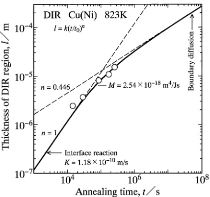
influences the rate-controlling process of the layer growth. Diffusion induced recrystallization (DIR) occurs in many metal systems. Here, DIR is the phenomenon that new fine grains with discontinuously different solute concentrations are formed behind moving grain boundaries owing to recrystallization combined with diffusion of solute atoms along the moving boundaries. Thefine-grain region produced by DIR is hereafter called the DIR region. The kinetics of DIR in the Cu(Ni) system was experimentally examined at
T=723823 K in a previous study,36) where the notation A(B) indicates that a solute B diffuses into a pure metal A or a binary AB alloy of the A-rich phase according to convention. The experimental result of T=823 K36) is represented as open circles in Fig. 8. In this figure, the ordinate shows the logarithm of the thickness l of the DIR region, and the abscissa indicates the logarithm of the annealing timet. In that study,36)the dependence oflontwas
[image:5.595.66.273.60.674.2]also theoretically calculated using a new extended (NE) model.37)The model calculation is shown as a solid curve in
Fig. 8. As can be seen, the solid curve is considered straight at t<104s in the early stages and at t>107s in the late
stages. In such cases,lis expressed as a power function oft
by eq. (3). In Fig. 8, the solid curve is extrapolated as dashed lines with n=1 and n=0.446 at t<104s and t>107s, respectively. From these values ofn, it is concluded that the growth of the DIR region is controlled by interface reaction in the early stages but by boundary diffusion in the late stages.36) In the intermediate stages for 104s<t<107s, however, the exponentngradually decreases with increasing annealing time t. Thus, the transition of the rate-controlling process occurs in the intermediate stages. For the transition, both interface reaction and boundary diffusion contribute to the rate-controlling process, and the contribution of boundary diffusion gradually increases with increasing annealing time. (a)
(b)
(c)
Fig. 6 The results in Fig. 4 are shown as open circles with solid lines: (a) T=433 K, (b) T=453 K, and (c) T=473 K. The corresponding results of the Au/Sn,21)Cu/Sn15)and Ni/Sn18)systems are indicated as open squares with dashed-and-dotted lines, open rhombuses with dashed lines and open triangles with dotted lines, respectively.
[image:5.595.316.536.66.283.2]As can be seen in Fig. 8, the open circles are distributed in the intermediate stages. Hence, the mixed rate-controlling process works within the experimental annealing times.
If eq. (3) is conveniently used to express the dependence oflontwithin the experimental annealing times, the values of k=5.86©10¹9m and n=0.630 are estimated from the
open circles in Fig. 8 by the least-squares method. Con-sequently, for the mixed rate-controlling process, the overall value ofn is smaller than unity but greater than 0.446. Also for the growth of the CoSn3layer in Fig. 4, the value ofncan
gradually decrease with increasing annealing time t. Unlike the growth of the DIR region, however, the contribution of boundary diffusion may not be important for the growth of the CoSn3 layer.9) As a result, the NE model37) cannot be
unfortunately applicable to the theoretical analysis of kinetics for the solid-state reactive diffusion in the Co/Sn system.
As shown in Fig. 7, n is rather insensitive to T. If n is considered to be independent of T, k and n in eq. (3) are simultaneously evaluated by the least-squares method from all the experimental points plotted in Fig. 4. The evaluated value ofnis shown as a solid circle with error bars in Fig. 7, and those ofkare indicated as open circles with error bars in Fig. 9. In Fig. 9, the ordinate shows the logarithm ofk, and the abscissa indicates the reciprocal ofT. The dependence of
konTis generally expressed by the following equation.21)
k¼k0exp RTQk
ð4Þ
Here,k0is the pre-exponential factor, andQkis the activation enthalpy. From the open circles in Fig. 9, k0 and Qk were evaluated by the least-squares method as shown with a solid line. The evaluated values are indicated in Fig. 9. The rate-controlling process of the layer growth is usually discussed on the value ofQk. As mentioned earlier, however, the layer growth of CoSn3atT=433473 K is controlled by volume
diffusion and interface reaction. Therefore, Qk contains
mixed-information on the temperature dependencies of volume diffusion and interface reaction. In such a case, the rate-controlling process cannot be estimated only from the value ofQk. It is worth noting thatnis much more useful than Qkfor the estimation of the rate-controlling process.
4. Conclusions
The reactive diffusion in the Co/Sn system was exper-imentally observed in a solid-state temperature range. In this experiment, the sandwich Sn/Co/Sn diffusion couple was prepared by a diffusion bonding technique and then isothermally annealed at temperatures of 433473 K for various periods up to 744 h. During annealing, an interme-tallic layer composed of CoSn3was produced at the original
interface in the diffusion couple. The mean thickness of the intermetallic layer is proportional to a power function of the annealing time. The exponent of the power function takes intermediate values between 0.5 and unity under the present annealing conditions. This means that both volume diffusion and interface reaction contribute to the rate-controlling process of the layer growth.
Acknowledgement
The present study was partially supported by a Grant-in-Aid for Scientific Research from the Ministry of Education, Culture, Sports, Science and Technology of Japan.
REFERENCES
1) K. Tanida, M. Umemoto, Y. Tomita, M. Tago, R. Kajiwara, Y. Akiyama and K. Takahashi:Jpn. J. Appl. Phys.42(2003) 21982203. 2) K. Tanida, M. Umemoto, N. Tanaka, Y. Tomita and K. Takahashi:Jpn.
J. Appl. Phys.43(2004) 22642270.
3) R. Labie: Dr. Thesis, Katholieke Universiteit Leuven, Leuven, (2007). 4) A. La Manna, T. Buisson, M. Detalle, K. J. Rebibis, D. Velenis, W. Zhang and E. Beyne: Proc. 62nd Electronic Components and Technology Conference, San Diego, (2012) p. 532.
5) W. Zhang, Z. Mai, L. Bogaerts, M. Gonzalez, G. Vakanas, A. Fig. 8 The thicknesslof the DIR region versus the annealing timetat
T=823 K for the Cu(Ni) system in a previous study.36)Open circles show the observation, and a solid curve indicates the calculation by the new extended (NE) model.37)The solid curve is extrapolated as dashed lines in the early and late stages of the reaction.
[image:6.595.315.536.65.274.2] [image:6.595.63.277.68.269.2]La Manna and E. Beyne: Proc. 4th Electronic System-Integration Technology Conference, Amsterdam, (2012) p. 1.
6) R. Labie, E. Beyne and P. Ratchev: Proc. 5th Electronics Packaging Technology, Singapore, (2003) p. 584.
7) R. Labie, P. Ratchev and E. Beyne: Proc. 55th Electronic Components and Technology Conference, Lake Buena Vista, (2005) p. 449. 8) S. Kim and J. Yu: Proc. Electronic Materials and Packaging, Taipei,
(2008) p. 313.
9) C. Wang and S. Chen:Intermetallics16(2008) 524530. 10) G. Humpston:J. Mater. Sci. Mater. Electron.21(2010) 584588. 11) C. Wang and C. Kuo:Mater. Chem. Phys.130(2011) 651656. 12) W. Zhang, A. La Manna, P. Soussan and E. Beyne: Proc. 3rd IEEE Int.
Workshop on Low Temperature Bonding for 3D Integration, Tokyo, (2012) p. 65.
13) Y. Liang, W. Tsao, C. Chen, D. Yao, A. Huang and Y. Lai:J. Appl.
Phys.111(2012) 043705.
14) C. Wang, C. Kuo, S. Huang and P. Li:Intermetallics32(2013) 5763. 15) T. Takenaka, S. Kano, M. Kajihara, N. Kurokawa and K. Sakamoto:
Mater. Sci. Eng. A396(2005) 115123.
16) M. Kajihara:Acta Mater.52(2004) 11931200.
17) A. Furuto and M. Kajihara:Mater. Trans.49(2008) 294303. 18) M. Mita, M. Kajihara, N. Kurokawa and K. Sakamoto:Mater. Sci. Eng.
A403(2005) 269275.
19) A. Lang and W. Jeitschko: Z. Metallkd.87(1996) 759764. 20) T. Takenaka, M. Kajihara, N. Kurokawa and K. Sakamoto:Mater. Sci.
Eng. A406(2005) 134141.
21) T. Yamada, K. Miura, M. Kajihara, N. Kurokawa and K. Sakamoto:
Mater. Sci. Eng. A390(2005) 118126.
22) M. Kajihara:Mater. Sci. Eng. A403(2005) 234240. 23) M. Kajihara:Defect. Diffus. Forum249(2006) 9196. 24) M. Kajihara:Mater. Trans.46(2005) 21422149. 25) M. Kajihara:Mater. Trans.47(2006) 14801484.
26) M. Kajihara and T. Yamashina:J. Mater. Sci.42(2007) 24322442. 27) M. Kajihara:Mater. Trans.49(2008) 715722.
28) M. Kajihara:J. Mater. Sci.44(2009) 21092118. 29) M. Kajihara:Mater. Trans.51(2010) 12421248. 30) M. Kajihara:Mater. Trans.53(2012) 18961904.
31) Y. Muranishi and M. Kajihara:Mater. Sci. Eng. A404(2005) 3341. 32) T. Hayase and M. Kajihara:Mater. Sci. Eng. A433(2006) 8389. 33) K. Mikami and M. Kajihara:J. Mater. Sci.42(2007) 81788188. 34) M. Kajihara and Y. Tejima:J. Phys. Conf. Ser.165(2009) 012091. 35) Y. Tejima, S. Nakamura and M. Kajihara:J. Mater. Sci.45(2010) 919
928.
36) Y. Yamamoto and M. Kajihara:J. Electron. Mater.37(2008) 1710 1720.