Reactive Diffusion between Ag and Sn at Solid State Temperatures
Ken Suzuki
1, Satoru Kano
1, Masanori Kajihara
2;*, Noriharu Kurokawa
3and Katsuhiko Sakamoto
3 1Graduate School, Tokyo Institute of Technology, Yokohama 226-8502, Japan2Department of Materials Science and Engineering, Tokyo Institute of Technology 3
Tyco Electronics AMP Co., Ltd., Kawasaki 214-8533, Japan
The reactive diffusion at solid-state temperatures was experimentally studied for the binary Ag–Sn system. Sn/Ag/Sn diffusion couples were prepared by a diffusion bonding technique and then annealed at temperatures betweenT¼433and 473 K for various periods in an oil bath with silicone oil. After annealing, layers of the"(Ag3Sn) andcompounds were observed to form at the Sn/Ag interface. Furthermore, a thin layer alloyed with Sn was produced into the Ag specimen from the/Ag interface owing to diffusion induced recrystallization (DIR). The thickness is about one order of magnitude greater for the"layer than for theand DIR layers. The total thicknesslof the"andlayers is described as a function of the annealing timetby the equationl¼kðt=t0Þn. Here,t0is unit time, 1 s. The exponentnis 0.40, 0.38 and 0.36 at
T¼433, 453 and 473 K, respectively. If the reactive diffusion is controlled by the volume diffusion,nis equal to 0.5. However,nis actually smaller than 0.5 at all the annealing temperatures. This indicates that the grain boundary diffusion contributes to the reactive diffusion and the grain growth occurs at certain rates. As the annealing temperature decreases, the contribution of the grain boundary diffusion should be more remarkable, but the grain growth will become sluggish. This is the reason why the value ofnincreases with decreasing annealing temperature.
(Received October 22, 2004; Accepted March 14, 2005; Published May 15, 2005)
Keywords: diffusion bonding, electron probe microanalysis, intermetallic compounds, bulk diffusion, solder
1. Introduction
Tin-base solder alloys are widely used to interconnect Cu-base conductor alloys in electronic industry. However, Cu– Sn intermetallic compounds are produced at the interface between the solder and conductor alloys during soldering and then soakingly grow owing to heating under usual energiza-tion condienergiza-tions.1–9) The Cu–Sn compounds are very brittle and possess high electrical resistivities. Hence, the growth of such compounds gradually deteriorates the electrical and mechanical properties of the interconnection. The Cu-base conductor alloy is usually plated with Au to improve the corrosion resistance. When the Au-plated conductor alloy is soldered with the Sn-base solder alloy, Au–Sn intermetallic compounds are formed at the interface. Like the Cu–Sn compounds, the Au–Sn compounds are brittle and possess high electrical resistivities. Thus, the growth of the Au–Sn compounds also causes the deterioration of the electrical and mechanical properties of the interconnection during heating. However, the growth rate is much faster for the Au–Sn compounds than for the Cu–Sn compounds.3,4,10–12)Thus, the Au plating remarkably accelerates the deterioration of the interconnection.
Recently, the reactive diffusion between Au and Sn at solid-state temperatures was experimentally observed by the present authors using Sn/Au/Sn diffusion couples prepared by a diffusion bonding technique.13–15)The diffusion couples were isothermally annealed at temperatures between T¼ 393and 473 K for various periods in an oil bath with silicone oil. Here, T is the annealing temperature. After annealing, compound layers composed of AuSn, AuSn2and AuSn4were observed to form at the Au/Sn interface in the diffusion couple. According to the observations, the total thickness of the compound layers is mathematically described as a power function of the annealing time, and the exponent of the power
function is 0.48, 0.42 and 0.36 atT ¼393, 433 and 473 K, respectively. Such temperature dependence of the exponent indicates that the grain boundary diffusion contributes to the rate-controlling process and grain growth occurs in the compound layers at certain rates at higher annealing temper-atures. As the annealing temperature decreases, the contri-bution of the grain boundary diffusion becomes remarkable, but the grain growth slows down.
In order to examine whether such a temperature depend-ency of the rate-controlling process is usually recognized in semblable binary systems, the reactive diffusion between Ag and Sn was experimentally observed in the present study. Sn/ Ag/Sn diffusion couples were prepared by the diffusion bonding technique and then isothermally annealed at
T ¼433{473K in the oil bath in a similar manner to previous studies.13–15) The growth behavior of Ag–Sn compound layers was metallographically observed, and then the rate-controlling process of the reactive diffusion was discussed.
2. Experimental
Polycrystalline pure Sn plates with a size of 125 2mm3were prepared by cold rolling and spark erosion from a commercial 1 kg rectangular ingot of pure Sn with purity of 99.997%. The cold-rolled Sn plates were separately annealed in evacuated silica capsules at 473 K for 2 h, followed by air cooling without breaking the capsules, and then chemically polished in an etchant composed of 20 vol% of hydrochloric acid, 20 vol% of nitric acid and 60 vol% of distilled water. The two surfaces with an area of 125mm2 of each chemically polished plate were mechanically polished on 1000 emery paper. One of the two surfaces was again mechanically polished on 1500 emery paper until a depth of 100mmand then finished using diamond with a diameter of 3mm.
Polycrystalline pure Ag plates with a dimension of *Corresponding author, E-mail: [email protected]
1042mm3were cut by spark erosion from a commer-cial 100 g rectangular bar of pure Ag with purity of 99.99% and then cold rolled to a thickness of 0.1 mm. Sheet specimens with a size of 2070:1mm3 were cut from the cold rolled specimens and then separately annealed in evacuated silica capsules at 1173 K for 2 h, followed by air cooling without breaking the capsules. The annealed sheet specimens were chemically polished in an etchant consisting of 10 vol% of nitric acid and 90 vol% of methanol.
After chemical polishing, a Ag sheet specimen was immediately sandwiched between two freshly prepared Sn plate specimens in methanol by a technique used in previous studies.13–15)The Sn/Ag/Sn couples were completely dried and then heat treated for diffusion bonding in the oil bath for 72 h atT¼433, 453 and 473 K. The diffusion couples were annealed at the same temperatures for various periods up to 1028 h. The summation of the heat-treating and annealing times is hereafter merely called the annealing time. Cross-sections of the annealed diffusion couples were mechanically polished using diamond with diameters of 15, 3 and 1mm, and then finished utilizing an OP-S liquid by Struers Ltd. The microstructure of the cross-section was observed with a differential interference contrast (DIC) optical microscope. Concentration profiles of Ag and Sn were determined on the cross-section along the direction normal to the interface by electron probe microanalysis (EPMA).
3. Results and Discussion
3.1 Growth behavior of compound layers
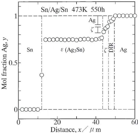
A typical DIC optical micrograph for the cross-section of the Sn/Ag/Sn diffusion couple is shown in Fig. 1. This figure indicates the micrograph of the diffusion couple annealed at 473 K for 550 h. As can be seen, slightly dark layers with a thickness of about 20mm are observed at both Sn/Ag interfaces on the upper and lower sides. In order to identify the dark layer, concentration profiles of Ag and Sn were measured by EPMA along the direction normal to the interface. A result for the diffusion couple in Fig. 1 is shown as open circles in Fig. 2. In this figure, the ordinate and the abscissa indicate the mol fraction of Ag and the distance, respectively. As can be seen in Fig. 2, two compound layers are recognized between the Sn and Ag specimens. They are the " (Ag3Sn) and phases on the Sn and Ag sides, respectively. According to a recent phase diagram in the binary Ag–Sn system,16)the"andphases are the only stable
intermetallic compounds. Furthermore, a thin layer alloyed with Sn is discerned in the Ag specimen adjacent to the phase. Such an alloyed layer was produced by diffusion induced recrystallization (DIR). The thickness is about 30, 3 and 3mmfor the",and DIR layers, respectively. DIR is the phenomenon that new fine grains with discontinuously different solute concentrations are formed behind moving grain boundaries owing to recrystallization combined with diffusion of solute atoms along the moving boundaries.17–19) The solubility range at T ¼473K16)is shown as thin solid lines for the Ag and phases in Fig. 2. As can be seen, the maximum concentration of Sn in the DIR layer is close to the solubility of Sn in the Ag phase. The tracer diffusion coefficient D for the volume diffusion of Sn in Ag is evaluated to be1:91023m2/s atT ¼473K.20)Using this value ofD, the penetration distancexof Sn in Ag was roughly estimated from the equationx2¼4Dt. The estimation gives a value ofx¼0:01mm. Thus, the thickness of the DIR layer is about 300 times greater than the penetration distance for the volume diffusion of Sn in the Ag specimen.
As already shown in Fig. 1, the compound layers are discriminable from the Ag and Sn specimens in the DIC optical micrograph of the cross-section. However, it was difficult to distinguish the " and layers. Thus, the total thickness l of the compound layers was evaluated by the following equation from the cross-sectional micrographs.
l¼A=w ð1Þ
The layer consisting of the " and layers is hereafter designated the intermetallic layer. In eq. (1), A andware the total area and the total length of the intermetallic layer, respectively, in the cross-section. The results at annealing temperatures ofT¼433, 453 and 473 K are plotted as open triangles, squares and circles, respectively, in Fig. 3. As can be seen in this figure, the total thickness l monotonically increases with increasing annealing timetat all the temper-atures. Furthermore, the plotted points at each annealing Fig. 1 DIC optical micrograph of cross-section for the Sn/Ag/Sn diffusion
couple annealed at 473 K for 550 h.
Fig. 2 Concentration profile of Ag across a dark layer formed between Sn and Ag in Fig. 1.
[image:2.595.311.540.71.291.2] [image:2.595.54.284.652.757.2]temperature lie well on a straight line. As a consequence,lis mathematically described as a function oftby the equation
l¼kðt=t0Þn: ð2Þ
Here,t0 is unit time, 1 s. It is adopted to make the ratiot=t0 dimensionless. The proportionality coefficientkhas the same dimension as the total thickness l, but the exponent n is dimensionless. The values ofkandnwere determined from the plotted points in Fig. 3 by a least-squares method. The determination gives k¼3:39108m and n¼0:404 at T ¼433K,k¼5:36108m andn¼0:384atT ¼453K, andk¼1:17107m and n¼0:364atT ¼473K. Using these values, the total thicknesslwas calculated as a function of the annealing timetfrom eq. (2). The results are shown as solid straight lines in Fig. 3. As can be seen, most of the experimental points at each annealing temperature are located well on the corresponding straight line.
The results atT ¼433and 473 K in Fig. 3 are represented as open circles with solid lines in Figs. 4(a) and (b), respectively. As already mentioned in Introduction, the reactive diffusion between Au and Sn was experimentally studied by the present authors13–15)using Sn/Au/Sn diffusion couples atT ¼393{473K. The experimental results for the total thicknesslof the AuSn, AuSn2 and AuSn4 compound layers at T ¼433 and 473 K are plotted as open squares against the annealing time t in Figs. 4(a) and (b), respec-tively. Here, dashed lines indicate the calculation by eq. (2) with k¼2:71107m and n¼0:415 at T ¼433K and that with k¼9:55107m and n¼0:362 at T ¼473K. Furthermore, the reactive diffusion between Cu and Sn was experimentally observed by Onishi and Fujibuchi.21)In their experiment, Cu/Sn diffusion couples were prepared also by a diffusion bonding technique and then annealed at
T ¼463{493K for various periods. Their observations show that Cu3Sn and Cu6Sn5 compound layers are formed at the interface during annealing. In this case, however,nis equal to
0.5 independently of T, whereas kvaries depending on T. From its temperature dependence,21) k¼8:73109 and 1:69108m are obtained atT ¼433 and 473 K, respec-tively. The calculations by eq. (2) with these values ofkand
nare indicated as dotted lines in Fig. 4. As can be seen, the open circles lie rather well not only on the solid line but also on the dotted line. However,nis slightly smaller for the solid line than for the dotted line. Therefore, the total thicknesslis almost identical for the Ag–Sn and Cu–Sn intermetallic layers at the present annealing times but the rate-controlling process for the growth is different between these intermetal-lic layers. On the other hand,nis almost identical for the Au– Sn and Ag–Sn intermetallic layers, butlis about one order of magnitude greater for the former intermetallic layer than for the latter intermetallic layer.
Fig. 3 The total thicknesslof the intermetallic layer versus the annealing timetfor the Sn/Ag/Sn diffusion couple at annealing temperatures of 433, 453 and 473 K. Straight lines indicate the calculations from eq. (2).
[image:3.595.53.283.70.289.2] [image:3.595.311.542.73.510.2]3.2 Rate controlling process
The values of the exponent nfor the Sn/Ag/Sn and Sn/ Au/Sn14,15) diffusion couples are plotted as open circles and squares, respectively, with error bars against the anneal-ing temperature T in Fig. 5. When the reactive diffusion is controlled by the volume diffusion of the constituent ele-ments in each phase, the exponentnis equal to 0.5. On the other hand, the grain boundary diffusion across the interme-tallic layer will govern the reactive diffusion at low temper-atures where the volume diffusion is practically frozen out. If the reactive diffusion is purely controlled by the grain boun-dary diffusion and grain growth takes place in the intermetal-lic layer according to the parabointermetal-lic law, the exponent takes a value ofn¼0:25.22)Here, the parabolic law means that the grain size in the intermetallic layer is proportional to the square root of the annealing time. According to the results for the Sn/Au/Sn diffusion couple, n is equal to 0.36 at
T ¼473K and increases with decreasing annealing temper-ature. AtT¼393K,nbecomes close to 0.5. Even if the re-active diffusion is purely controlled by the grain boundary diffusion,nis equal to 0.5 unless the grain growth occurs.15) Hence, for the reactive diffusion between Au and Sn, the grain boundary diffusion contributes to the rate-controlling process, and the grain growth takes place at a certain rate atT ¼473K. However, atT¼393K, the grain growth will slow down, though the contribution of the grain boundary diffusion becomes more remarkable.15) As can be seen in Fig. 5, the open circles well coincide with the open squares. This indicates that the same rate-controlling process as the re-active diffusion between Au and Sn works also in the rere-active diffusion between Ag and Sn at each annealing temperature. The values of the logarithm of k are plotted against the reciprocal ofT as open circles with error bars in Fig. 6. As can be seen, the open circles are located well on a straight line. This means thatkis expressed as a function ofT by the equation
k¼k0expðQk=RTÞ: ð3Þ
Here, k0 is the pre-exponential factor, Qk is the activation enthalpy, andRis the gas constant. From the open circles in Fig. 6,k0 andQkwere evaluated by a least-squares method. The evaluation provides k0 ¼7:10102m and Qk¼ 52:6kJ/mol. Using these parameters, the temperature de-pendence of k was calculated from eq. (3). The result is shown as a solid line in Fig. 6. In this figure, the corresponding results for the Sn/Au/Sn14,15) and Cu/Sn21) diffusion couples are indicated as open squares with a dashed line and open triangles with a dotted line, respectively. According to the results in Fig. 5,nis almost identical for the Sn/Ag/Sn and Sn/Au/Sn diffusion couples at each anneal-ing temperature. However,lis one order of magnitude greater for the Sn/Au/Sn diffusion couple than for the Sn/Ag/Sn diffusion couple as shown in Fig. 4. Therefore,kis also one order of magnitude greater for the former diffusion couple than for the latter diffusion couple. On the other hand, l is close to each other for the Sn/Ag/Sn and Cu/Sn diffusion couples at the present annealing times, butnis smaller for the former diffusion couple than for the latter diffusion couple. As a result,k becomes greater for the Sn/Ag/Sn diffusion couple than for the Cu/Sn diffusion couple. The rate-controlling process varies depending on the annealing temperature for the reactive diffusion between Ag and Sn and that between Au and Sn as mentioned earlier. Thus, complex information for the temperature dependencies of the volume diffusion, the grain boundary diffusion and the grain growth in each phase is included in the activation enthalpy
Qk. In order to account for the physical meaning ofQk, these temperature dependencies should be know separately. Un-fortunately, however, such information is not available for the Sn/Ag/Sn and Sn/Au/Sn diffusion couples. Conse-quently, it is not appropriate to estimate the rate-controlling process only from the value ofQk.
Fig. 5 The exponentnversus the annealing temperatureTfor the Sn/Ag/ Sn diffusion couple. Open squares indicate the results for the Sn/Au/Sn diffusion couple by the present authors.14,15)
Fig. 6 The proportionality coefficient k versus the reciprocal of the annealing temperatureT. Open squares show the results for the Sn/Au/Sn diffusion couple by the present authors,14,15)and open triangles indicate those for the Cu/Sn diffusion couple by Onishi and Fujibuchi.21)Straight lines exhibit the calculations from eq. (3).
[image:4.595.53.287.62.294.2] [image:4.595.310.543.71.288.2]4. Conclusions
The kinetics of the reactive diffusion between Ag and Sn was experimentally examined at solid-state temperatures using Sn/Ag/Sn diffusion couples. The diffusion couples were prepared by a diffusion bonding technique and then annealed at temperatures of T ¼433 to 473 K for various periods in the oil bath with silicone oil. Owing to annealing, the"(Ag3Sn) andcompound layers are formed at the Sn/ Ag interface in the diffusion couple. In the Ag specimen adjacent to the layer, a thin layer alloyed with Sn is produced by diffusion induced recrystallization (DIR). Thickness of the DIR layer is close to that of the layer but one tenth of that of the"layer. The total thicknesslof the compound layers monotonically increases with increasing annealing timetaccording to the equationl¼kðt=t0Þn, where t0 is unit time, 1 s. The proportionality coefficientkand the exponentnwere determined from the experimental results by a least-squares method. The determination provides k¼ 3:39108m and n¼0:404 at T ¼433K, k¼5:36 108m andn¼0:384atT¼453K, andk¼1:17107m andn¼0:364atT ¼473K. Such a temperature dependency of the exponentnindicates that the grain boundary diffusion contributes to the reactive diffusion and the grain growth occurs at certain rates at higher annealing temperatures. At lower annealing temperatures, however, the grain boundary diffusion becomes more predominant, but the grain growth will slow down. This type of rate-controlling process has been observed also for the reactive between Au and Sn.14,15)
Acknowledgements
The authors are grateful to Mr. K. Miura at Tokyo Institute of Technology, Japan for assistance at early stages of the present study. The study was supported by Tyco Electronics AMP Co., Ltd., Japan.
REFERENCES
1) L. Zakraysek: Welding Research Supplement Nov. (1972) 536–541. 2) K. N. Tu: Acta Metall.21(1973) 347–354.
3) H. N. Keller: IEEE Trans. Components, Hybrids, Manuf. Tech. CHMT-2 (1979) 180–195.
4) H. N. Keller and J. M. Morabito: Surface and Interface Analysis3 (1981) 16–22.
5) J. O. G. Parent, D. D. L. Chung and I. M. Bernstein: J. Mater. Sci.23 (1988) 2564–2572.
6) A. J. Sunwoo, J. W. Morris Jr. and G. K. Lucey Jr.: Metall. Trans.23A (1992) 1323–1332.
7) P. T. Vianco, P. F. Hlava and A. L. Kilgo: J. Elect. Mater.23(1994) 583–594.
8) D. R. Frear and P. T. Vianco: Metall. Trans.25A(1994) 1509–1523. 9) S. Choi, T. R. Bieler, J. P. Lucas and K. N. Subramanian: J. Elect.
Mater.28(1999) 1209–1215.
10) E. I.-B. Hannech and C. R. Hall: Mater. Sci. Tech.8(1992) 817–824. 11) H. N. Keller: IEEE Trans. Components, Hybrids, Manuf. Tech.
CHMT-5 (1982) 408–419.
12) C. Wright: IEEE Trans. Parts, Hybrids, Packaging PHP-13 (1977) 202– 207.
13) M. Kajihara, T. Yamada, K. Miura, N. Kurokawa and K. Sakamoto: Netsushori43(2003) 297–298.
14) T. Yamada, K. Miura, M. Kajihara, N. Kurokawa and K. Sakamoto: J. Mater. Sci.39(2004) 2327–2334.
15) T. Yamada, K. Miura, M. Kajihara, N. Kurokawa and K. Sakamoto: Mater. Sci. Eng. A390(2005) 118–126.
16) T. B. Massalski, H. Okamoto, P. R. Subramanian and L. Kacprzak: Binary Alloy Phase Diagram (ASM International, Materials Park, OH, 1990) vol. 1, p. 96.
17) M. Kajihara and W. Gust: Acta Metall. Mater.39(1991) 2565–2574. 18) Y. Kawanami, M. Nakano, M. Kajihara and T. Mori: Mater. Trans. JIM
39(1998) 218–224.
19) Y. Yamamoto and M. Kajihara: Mater. Trans.42(2001) 1763–1770. 20) Metals Data Book, ed. Japan Institute of Metals (Maruzen, Tokyo,
1993) p. 20.
21) M. Onishi and H. Fujibuchi: Trans. JIM16(1975) 539–547. 22) Y. L. Corcoran, A. H. King, N. de Lanerolle and B. Kim: J. Electron.