Kinetics of Solid-State Reactive Diffusion in the (Sn
Ni)
/
Cu System
Misako Nakayama
1and Masanori Kajihara
2,+1Graduate School, Tokyo Institute of Technology, Yokohama 226-8502, Japan
2Department of Materials Science and Engineering, Tokyo Institute of Technology, Yokohama 226-8502, Japan
The kinetics of the solid-state reactive diffusion between SnNi alloys and pure Cu was experimentally observed to examine effects of addition of Ni into Sn on the growth behavior of compounds at the interconnection between the Sn-base solder and the multilayer Au/Ni/Cu conductor during energization heating. In this experiment, sandwich (SnNi)/Cu/(SnNi) diffusion couples with Ni concentrations ofy=0.01 and 0.03 were isothermally annealed in the temperature range of 433473 K for various periods up to 1152 h, whereyis the mol fraction of Ni. After annealing, a compound layer consisting of Cu6Sn5and Cu3Sn was recognized between the SnNi alloy and the Cu specimen in the diffusion couple. Here, the thickness of the Cu3Sn layer is smaller than that of the Cu6Sn5layer. The (Cu,Ni)6Sn5grains were transformed from the Ni3Sn4grains in the SnNi alloy in the neighborhood of the Cu6Sn5layer, and then adhered to the Cu6Sn5layer. The overall growth of the compound layer including the (Cu,Ni)6Sn5grains is remarkably accelerated by the adhesion, but that of the compound layer excluding the (Cu,Ni)6Sn5grains is slightly decelerated by the adhesion. The mean thickness of each layer increases in proportion to a power function of the annealing time. For annealing at 433473 K, the ratio between the thicknesses of the Cu6Sn5and Cu3Sn layers is hardly affected by the addition of Ni into Sn up toy=0.03. [doi:10.2320/matertrans.M2014038]
(Received February 4, 2014; Accepted May 16, 2014; Published July 4, 2014)
Keywords: reactive diffusion, metallization, solder, conductor, intermetallic compounds
1. Introduction
Owing to high electrical conductivity, Cu-base alloys are widely used as conductor materials in the electronics industry. If the Cu-base conductor is interconnected with a Sn-base solder, Cu6Sn5 and Cu3Sn are formed at the interconnection between the conductor and the solder during soldering and then gradually grow during energization heating at solid-state temperatures.111) Since the CuSn compounds are brittle and possess high electrical resistivities, their growth deteriorates the mechanical and electrical properties of the interconnection. To inhibit the formation of the compounds, the Cu-base conductor is usually plated with a Ni layer. However, Ni is not sufficiently corrosion resistant. Thus, the Ni layer is plated with a Au or Pd layer to improve corrosion resistance.1215)
For the multilayer Au/Ni/Cu conductor with a thin Au layer, the Au layer quickly dissolves into a molten Sn-base solder during soldering, and then the Ni layer is contacted with the solder. Consequently, the Ni layer is directly reacted with the solder during solid-state energization heating. The solid-state reactive diffusion in the Ni/Sn system was experimentally examined using sandwich Sn/Ni/Sn diffu-sion couples prepared by a diffudiffu-sion bonding technique in a previous study.16) In this experiment, the diffusion couples were isothermally annealed at temperatures of T=433 473 K. At the interface in the annealed diffusion couple, a layer of Ni3Sn4was observed atT=453473 K, but granular particles of Ni3Sn4were recognized atT=433 K. The mean thickness of the Ni3Sn4 layer increases in proportion to a power function of the annealing time. The exponent of the power function is 0.46 and 0.41 at T=453 and 473 K, respectively. The exponent smaller than 0.5 indicates that the growth of Ni3Sn4 is controlled by boundary and volume diffusion and grain growth occurs in Ni3Sn4. Although the growth of Ni3Sn4may be accelerated by boundary diffusion,
the overall growth rate is smaller for Ni3Sn416) than for Cu6Sn5and Cu3Sn.3,11)As a consequence, the Ni layer works as a barrier against the reactive diffusion at the interconnec-tion between the Sn-base solder and the multilayer Au/ Ni/Cu conductor with a thin Au layer during solid-state energization heating.
After prolonged energization heating, however, the Ni layer will be completely depleted by the growth of Ni3Sn4. Due to the depletion of the Ni layer, the Cu-base conductor is directly contacted with the solder. In such a case, the reactive diffusion between the conductor and the solder occurs at the interconnection. The solid-state reactive diffusion in the Cu/Sn system was experimentally observed in a previous study.11)In this experiment, like the Ni/Sn system,16)Sn/Cu/ Sn diffusion couples were prepared by a diffusion bonding technique and then isothermally annealed atT=433473 K. At all the annealing temperatures, an intermetallic layer composed of Cu6Sn5and Cu3Sn is formed at the original Cu/ Sn interface in the diffusion couple. Also in this case, the intermetallic layer grows according to the power relationship. The exponent of the power function is close to 0.5 at T=
473 K but becomes 0.37 and 0.43 at T=433 and 453 K, respectively. Thus, in the Cu/Sn system,11)the growth of the intermetallic layer is controlled by volume diffusion at
T=473 K but by volume and boundary diffusion atT=433 and 453 K. Therefore, the rate-controlling process of reactive diffusion varies depending on the annealing temperature and the metal system.
As previously mentioned, during prolonged energization heating, the Ni layer of the multilayer Au/Ni/Cu conductor is entirely consumed by the growth of Ni3Sn4, and then the Cu-base conductor is reacted with the Sn-base solder dispersed with Ni3Sn4. The dispersion of Ni3Sn4 in the solder may influence the kinetics of the reactive diffusion between the conductor and the solder at the interconnection. Unfortunately, however, reliable information on such infl u-ence is rather limited. To examine this influence, the kinetics of the solid-state reactive diffusion in the (SnNi)/Cu system +Corresponding author, E-mail: kajihara@materia.titech.ac.jp
was experimentally observed at temperatures of T=433 473 K using sandwich (SnNi)/Cu/(SnNi) diffusion cou-ples with Ni mol fractions of 0.010.03 in the present study.
2. Experimental
Binary SnNi alloys with Ni concentrations of y=0.01 and 0.03 were made as 25 g button ingots by argon arc melting from pure Sn and Ni with purities of 99.99 and 99.97%, respectively, whereyis the mol fraction of Ni. Plate specimens with a size of 12 mm©5 mm©2 mm were prepared by cold rolling and spark erosion from the button ingots. The plate specimens were isothermally heated in an oil bath with silicone oil at 473 K for 2 h, followed by water quenching. The two surfaces with an area of 12 mm©5 mm of each heated SnNi plate specimen were mechanically polished on # 800 emery paper. One of the two polished surfaces was again mechanically polished on # 15004000 emery papers until a depth of 100 µm and thenfinished using diamond with a diameter of 1 µm.
Sheet specimens with a size of 20 mm©7 mm©0.2 mm were cut from a pure Cu commercial sheet with dimensions of 300 mm©100 mm©0.2 mm and purity of 99.96% and then separately annealed in evacuated silica capsules at 1173 K for 2 h, followed by air cooling without breaking the capsules. The annealed sheet specimens were chemically polished in nitrohydrochloric acid for 60 s.
After chemical polishing, a Cu sheet specimen was immediately sandwiched between the finished surfaces of two freshly prepared SnNi plate specimens in ethanol by the technique used in a previous study.11) The sandwich (Sn Ni)/Cu/(SnNi) couples were completely dried and then heat treated for diffusion bonding in the oil bath at 433 K, 453 K and 473 K for 12.5 h. After the heat treatment, the diffusion couples were isothermally annealed at 433 K, 453 K and 473 K for various times up to 1139.5 h. The summation of the heat-treating and annealing times is hereafter merely called the annealing time t, and the annealing temperature is denoted by T. The chemical composition of the SnNi alloy is described as SnyNi. The Sn0.01Ni and Sn0.03Ni alloys are designated alloys N1 and N2, respectively, and the diffusion couples with alloys N1 and N2 are called diffusion couples N1 and N2, respectively. Cross-sections of the annealed diffusion couple were mechanically polished using diamond with diameters of 15, 3 and 1 µm, and then finished with an OP-S liquid manufactured by Struers Ltd. The microstructure of the cross-section was observed by differential interference contrast optical microscopy (DICOM). Concentrations of Sn, Ni and Cu in each phase on the cross-section were measured by electron probe microanalysis (EPMA).
3. Results and Discussion
3.1 Microstructure
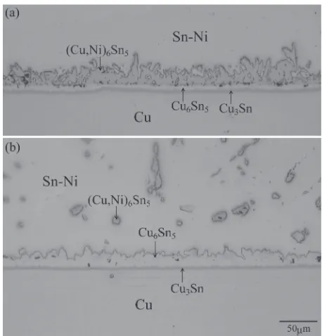
Typical DICOM images for the cross-section of diffusion couple N1 with T=473 K and t=144 h (5.18©105s) are shown in Fig. 1. For each DICOM image in Fig. 1, the top and bottom regions are the SnNi alloy and the Cu specimen,
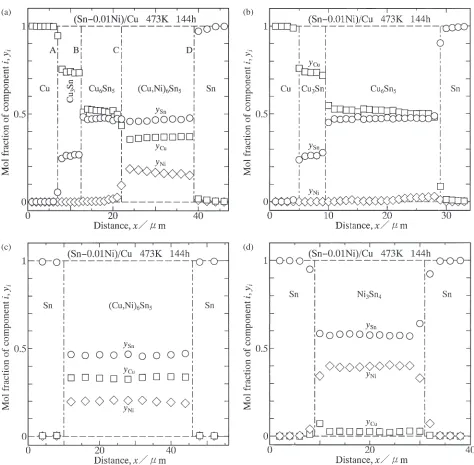
respectively. As can be seen, layers with different contrasts are formed at the original (SnNi)/Cu interface. To identify each layer, concentration profiles of Sn, Ni and Cu were measured by EPMA along the direction normal to the original interface. Results of the layers in Fig. 1(a) and 1(b) are indicated in Fig. 2(a) and 2(b), respectively. In Fig. 2, the ordinate and the abscissa show the mol fraction yi of
component i and the distance xmeasured from an arbitrary origin, respectively, and open circles, rhombuses and squares represent the mol fractionsySn,yNi andyCu, respectively. In Fig. 2(b), the layers on the SnNi and Cu sides are Cu6Sn5 and Cu3Sn, respectively. The thickness is much smaller for Cu3Sn than for Cu6Sn5. On the other hand, in Fig. 2(a), (Cu,Ni)6Sn5 is recognized on the SnNi side of the Cu6Sn5layer. Here, the Cu/Cu3Sn, Cu3Sn/Cu6Sn5, Cu6Sn5/ (Cu,Ni)6Sn5 and (Cu,Ni)6Sn5/Sn interfaces are denoted by interfaces A, B, C and D, respectively. The thickness of the Cu6Sn5 layer is smaller in Figs. 1(a) and 2(a) with (Cu,Ni)6Sn5than in Figs. 1(b) and 2(b) without (Cu,Ni)6Sn5. The EPMA measurement was conducted also for compound grains dispersed in the SnNi alloy of the diffusion couple shown in Fig. 1. Figure 2(c) indicates the result of a compound grain near by the Cu6Sn5+Cu3Sn two-phase layer, and Figure 2(d) represents that of a compound grain far from the two-phase layer. The compound grain in the SnNi alloy is originally Ni3Sn4as shown in Fig. 2(d). In Fig. 2(c), however, Ni3Sn4transforms into (Cu,Ni)6Sn5by diffusion of Cu from the Cu specimen to the SnNi alloy across the compound layers. The (Cu,Ni)6Sn5grains remain separately in Fig. 1(b) but adhere to the Cu6Sn5 layer in Fig. 1(a). In diffusion couples N1 and N2 annealed atT=433473 K, the microstructure type of Fig. 1(a) was observed predominantly, and that of Fig. 1(b) was recognized partially.
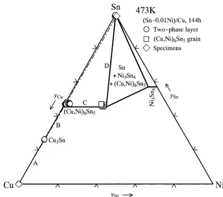
[image:2.595.312.541.68.307.2]solid-state temperatures in a previous study.17)The isothermal section at T=473 K of the phase diagram in this ternary system is shown in Fig. 3. As can be seen, a three-phase equilibrium of Sn+(Cu,Ni)6Sn5+Ni3Sn4 appears at this temperature. According to the tie-triangle of this three-phase equilibrium, the solubilityyCu6Sn5
Ni of Ni in Cu6Sn5is 0.224, and thatyNi3Sn4
Cu of Cu in Ni3Sn4 is 0.046.17)Thus, yNiCu3Sn4 is much smaller than yCu6Sn5
Ni . Therefore, in Fig. 3, Cu6Sn5 is described as (Cu,Ni)6Sn5, but Ni3Sn4 is merely expressed as Ni3Sn4. In Fig. 3, the concentration profiles for the two-phase layer and the (Cu,Ni)6Sn5 grain in Fig. 2 are plotted as diffusion paths with open circles and squares, respectively. For the two-phase layer, the open circles are located in the neighborhood of the binary SnCu side. In contrast, for the (Cu,Ni)6Sn5 grain, the open squares lie almost on the (Cu,Ni)6Sn5 corner of the three-phase tie-triangle. Thus, the concentration of Ni in the (Cu,Ni)6Sn5 grain reaches the solubility limit.
3.2 Growth behavior of intermetallic layer
As shown in Fig. 1(a), a multi-phase layer consisting of (Cu,Ni)6Sn5, Cu6Sn5 and Cu3Sn formed at the original (Sn Ni)/Cu interface in diffusion couples N1 and N2 due to isothermal annealing atT=433473 K. Hereafter, the multi-phase layer is merely called the intermetallic layer. From DICOM images, such as that indicated in Fig. 1(a), the area
Aj of the intermetallic layer corresponding to the partial
lengthwiof the original (SnNi)/Cu interface were measured
for cross-section j. The sumsAand wwere obtained by the equations11)
A¼Xm j¼1
Aj (1a)
and
w¼Xm j¼1
wj (1b)
(a) (b)
(c) (d)
[image:3.595.60.534.64.529.2]fromAiandwi, respectively, wherewj=422 µm andm²5.
Using the values of A and w, the total thickness l of the intermetallic layer was evaluated at each annealing time tas follows:11)
l¼Aw: ð2Þ
The results of diffusion couples N0,11)N1 and N2 are shown as open circles, squares and rhombuses, respectively, in Fig. 4. Here, diffusion couple N0 stands for the Sn/Cu/Sn diffusion couple from a previous study.11)Figure 4(a), 4(b) and 4(c) shows the results for T=433, 453 and 473 K, respectively. In this figure, the ordinate and the abscissa indicate the logarithms of l and t, respectively. As can be seen, the thicknesslmonotonically increases with increasing annealing time t. Furthermore, at T=433473 K, the experimental points for each diffusion couple lie well on a straight line. Consequently,lis expressed as a power function of tas follows
l¼k tt 0
n
; ð3Þ
where t0 is unit time, 1 s, which is adopted to make the argument t/t0 of the power function dimensionless. The proportionality coefficientk has the same dimension as the thickness l, and the exponent n is dimensionless. From the experimental points in Fig. 4,kandnwere evaluated by the least-squares method as indicated with various straight lines. The evaluated values of k and n are also shown in Fig. 4. According to the evaluation at T=433473 K, the overall growth rate of the intermetallic layer considerably increases with increasing Ni concentration ywithin the experimental annealing times.
3.3 Growth behavior of two-phase layer
According to Fig. 1(a), each compound is clearly distin-guished in the intermetallic layer. From DICOM images, such as that shown in Fig. 1(a), the mean thicknessliof compound
Fig. 3 Diffusion paths for the concentration profiles of the Cu6Sn5 and Cu3Sn layers and the (Cu,Ni)6Sn5grain in Fig. 2 shown as open circles and squares, respectively.
(a)
(b)
(c)
[image:4.595.312.542.55.758.2] [image:4.595.52.282.68.271.2]layer i in the intermetallic layer was evaluated using the relationships similar to eqs. (1a), (1b) and (2), where i=3 and 6 for the Cu3Sn and Cu6Sn5layers, respectively. The total thicknesslsof the Cu3Sn and Cu6Sn5layers was calculated by the equation
ls¼l3þl6: ð4Þ
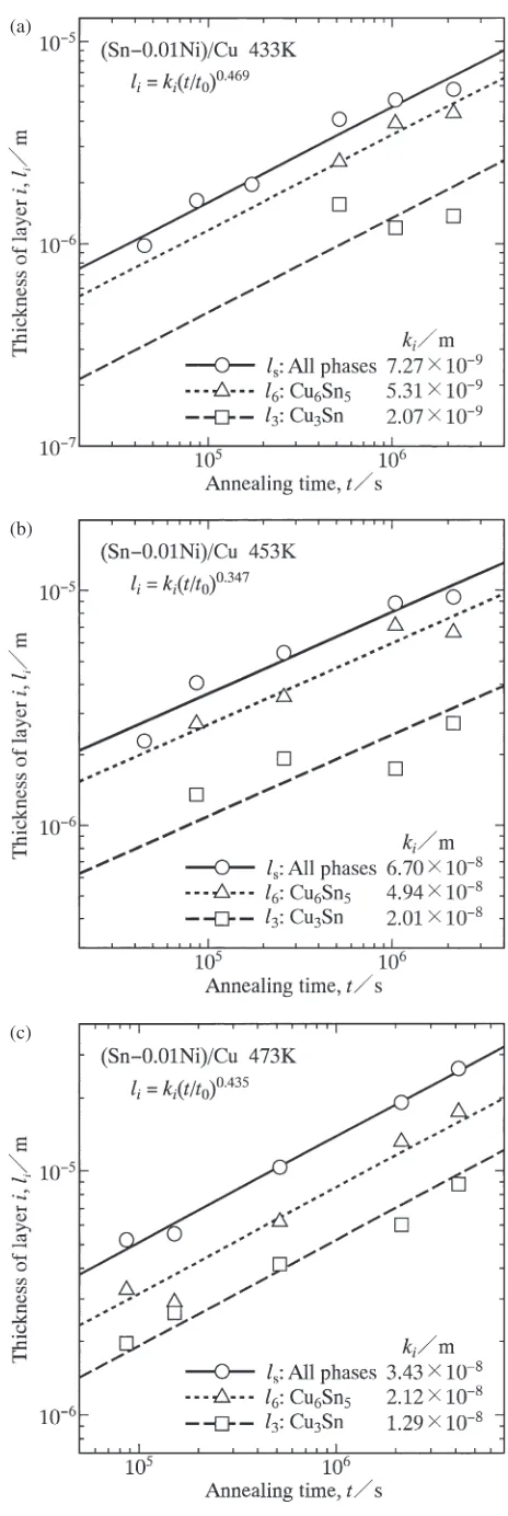
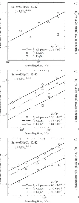
The Cu3Sn+Cu6Sn5 two-phase layer excluding the (Cu,Ni)6Sn5 grains from the intermetallic layer is hereafter denominated the two-phase layer. The results ofls,l6and l3 are shown as open circles, triangles and squares, respectively, in Figs. 5 and 6. In thesefigures, like Fig. 4, the ordinate and the abscissa indicate the logarithms ofli andt, respectively.
Figure 5(a), 5(b) and 5(c) shows the results for diffusion couple N1 at T=433, 453 and 473 K, respectively, and Fig. 6(a), 6(b) and 6(c) represents those for diffusion couple N2 at T=433, 453 and 473 K, respectively. Although the open squares are slightly scattered due to small values of l3, most of the open symbols are located well on the corresponding straight line. Therefore, we consider that liis
expressed as a power function oftby the following equation of the same formula as eq. (3).
li¼ki tt
0
n
ð5Þ
From the experimental points in Figs. 5 and 6,ksandnforls in eq. (5) were evaluated by the least-squares method as shown with solid lines. Sincel3andl6are smaller thanls, the values ofk3,k6andn forl3and l6cannot be estimated with the same reliability as those ofksandnforls. Consequently, using the same value of n as ls, k3 and k6 for l3 and l6 in eq. (5) were estimated from the open squares and triangles by the least-squares method as indicated with dashed and dotted lines, respectively. The values ofn,ks,k3andk6are shown in Figs. 5 and 6. Sincel3is very small for diffusion couple N2 atT=433 K,l3and thusl6could not be reliably determined for most of the annealing times except the longest time of
t=1152 h (4.15©106s) in Fig. 6(a). Therefore, k3 and k6 were not evaluated for diffusion couple N2 atT=433 K. As can be seen,l3is smaller thanl6for diffusion couples N1 and N2 atT=433473 K. Although the identical value ofnwas adopted for each diffusion couple at each annealing temper-ature, k3, k6 andks were independently evaluated from the corresponding experimental points in Figs. 5 and 6 as mentioned earlier. As a result, the relationship ks=k3+k6 does not necessarily hold, even though equation (4) holds at each experimental annealing time.
The values oflsin Figs. 5 and 6 are again plotted against the annealing timetin Fig. 7. In thisfigure, the correspond-ing result of diffusion couple N011) in Fig. 4 is also shown. Figure 7(a), 7(b) and 7(c) indicates the results for T=433, 453 and 473 K, respectively, and open circles, squares and rhombuses represent the results of diffusion couples N0,11) N1 and N2, respectively. Unlikelin Fig. 4,lsrather gradually decreases with increasing Ni concentration y within the experimental annealing times at each annealing temperature in Fig. 7. As mentioned in Section 3.1, Ni3Sn4in the SnNi alloy transforms into (Cu,Ni)6Sn5 owing to diffusion of Cu from the Cu specimen to the SnNi alloy across the two-phase layer. After transformation, (Cu,Ni)6Sn5grains mainly
(a)
(b)
(c)
[image:5.595.310.542.64.756.2](a)
(b)
(c)
Fig. 6 The thicknessesls,l6andl3in eq. (4) versus the annealing timet for diffusion couple N2 shown as open circles, triangles and squares, respectively: (a) 433 K, (b) 453 K and (c) 473 K.
(a)
(b)
(c)
[image:6.595.62.330.64.750.2] [image:6.595.294.537.68.750.2]adhere to the Cu6Sn5layer as shown in Fig. 1(a). The grain size is greater for the (Cu,Ni)6Sn5 grains adhered to the Cu6Sn5 layer than for those isolated in the SnNi alloy. According to the same mechanism as Ostwald ripening,18)the coarse (Cu,Ni)6Sn5 grains grow, but the fine (Cu,Ni)6Sn5 grains shrink. As a consequence, the adhesion of (Cu,Ni)6Sn5 spontaneously proceeds during isothermal annealing. Although the adhesion directly contributes to the increase in the thicknessl of the intermetallic layer, it consumes the Cu atoms transported from the Cu specimen across the phase layer as indicated in Fig. 2(a). The growth of the two-phase layer will be decelerated by the consumption of the Cu atoms. This is the reason why the increase in the Ni concentration y accelerates the overall growth of the intermetallic layer as shown in Fig. 4 but decelerates that of the two-phase layer as indicated in Fig. 7.
At each experimental annealing time, the ratioriof the
thick-nesslito the total thicknesslswas evaluated by the equation
ri¼lli
s: ð6Þ
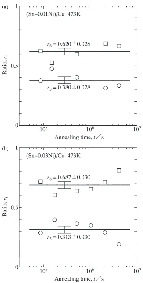
The values of r3 andr6 atT=473 K are plotted against the annealing timetas open circles and squares, respectively, in Fig. 8. Figure 8(a) and 8(b) shows the results of diffusion couples N1 and N2, respectively. As indicated in Figs. 5 and 6,l3 is smaller thanl6. Consequently,r3 is smaller than 0.5, but r6 is greater than 0.5. Although the open symbols are slightly scattered in Fig. 8, there exists no systematic dependence of ri on t. Thus, we may consider that ri is
constant independent of t for each diffusion couple. The mean values ofr3andr6were estimated from the open circles and squares, respectively, as shown as horizontal solid lines with error bars in Fig. 8. Here, the error bar indicates the standard error. The mean values of r3 and r6 are plotted against the Ni concentration yas open circles and squares, respectively, with error bars in Fig. 9. In this figure, the corresponding results ofr3andr6fory=011)are also shown as open circles and squares, respectively, with error bars. Furthermore, their mean values for y=0 are emphasized with horizontal solid lines. As can be seen, the values of r3 and r6 aty=0.03 are almost equal to those ofr3 and r6 at
y=0, respectively, and there are no systematic dependencies of r3and r6 ony. Thus, we may consider that r3 andr6 are constant independent ofy. As a consequence, it is concluded that the addition of Ni into Sn up to 3 at%slightly decelerates the overall growth of the Cu6Sn5and Cu3Sn layers but hardly influences the ratio of their thicknesses.
4. Conclusions
The solid-state reactive diffusion in the (SnNi)/Cu system was experimentally observed using the (SnNi)/
(a)
(b)
Fig. 8 The ratios r3 and r6 in eq. (6) versus the annealing time t at T=473 K shown as open circles and squares, respectively, with error bars: (a) diffusion couple N1, and (b) diffusion couple N2.
[image:7.595.52.286.65.527.2] [image:7.595.310.543.70.299.2]Cu/(SnNi) diffusion couples with Ni mol fractions of
y=0.01 and 0.03. The diffusion couples were isothermally annealed at temperatures of T=433, 453 and 473 K for various times up to t=1152 h. During annealing, the Cu6Sn5+Cu3Sn two-phase layer forms at the original (Sn Ni)/Cu interface in the diffusion couple, where the thickness is smaller for the Cu3Sn layer than for the Cu6Sn5layer. The Ni3Sn4grains in the SnNi alloy near by the two-phase layer transform into (Cu,Ni)6Sn5 and adhere to the Cu6Sn5 layer. Although the adhesion of (Cu,Ni)6Sn5 considerably accel-erates the overall growth of the (Cu,Ni)6Sn5+Cu6Sn5+ Cu3Sn layer, it slightly decelerates that of the Cu6Sn5+ Cu3Sn layer. The mean thickness of each compound layer is proportional to a power function of the annealing time. The addition of Ni into Sn within y=00.03 hardly influences the ratio between the thicknesses of the Cu6Sn5 and Cu3Sn layers atT=433473 K.
Acknowledgements
The authors are grateful to Mr. K. Sakamoto and Mr. N. Kurokawa at Tyco Electronics AMP Co. Ltd., Japan for stimulating discussions. The present study was supported by the Iketani Science and Technology Foundation in Japan. The study was also partially supported by a Grant-in-Aid for Scientific Research from the Ministry of Education, Culture, Sports, Science and Technology of Japan.
REFERENCES
1) L. Zakraysek: Welding Res. Suppl. Nov. (1972) 536541. 2) K. N. Tu:Acta Metall.21(1973) 347354.
3) M. Onishi and H. Fujibuchi: Trans. JIM16(1975) 539547. 4) H. N. Keller:IEEE Trans. Components Hybrids Manuf. Tech.
CHMT-2(1979) 180195.
5) H. N. Keller and J. M. Morabito:Surf. Interface Anal.3(1981) 1622.
6) J. O. G. Parent, D. D. L. Chung and I. M. Bernstein:J. Mater. Sci.23
(1988) 25642572.
7) A. J. Sunwoo, J. W. Morris, Jr. and G. K. Lucey, Jr.:Metall. Trans. A
23(1992) 13231332.
8) P. T. Vianco, P. F. Hlava and A. L. Kilgo:J. Electron. Mater.23(1994) 583594.
9) D. R. Frear and P. T. Vianco:Metall. Trans. A25(1994) 15091523.
10) S. Choi, T. R. Bieler, J. P. Lucas and K. N. Subramanian:J. Electron. Mater.28(1999) 12091215.
11) T. Takenaka, S. Kano, M. Kajihara, N. Kurokawa and K. Sakamoto:
Mater. Sci. Eng. A396(2005) 115123.
12) C. Wright:IEEE Trans. Parts, Hybrids, PackagingPHP-13(1977) 202 207.
13) H. N. Keller: IEEE Trans. Components, Hybrids, Manuf. Tech.
CHMT-5(1982) 408419.
14) E. I.-B. Hannech and C. R. Hall:Mater. Sci. Tech.8(1992) 817824.
15) G. Ghosh:Acta Mater.48(2000) 37193738.
16) M. Mita, M. Kajihara, N. Kurokawa and K. Sakamoto:Mater. Sci. Eng. A403(2005) 269275.
17) W. Shinmei: Master Thesis, Tokyo Inst. Tech. (2013).