~~~OO@[P@~~~
[ID~~ill
~@IT\!]uOO@~~~OO
[lli@illOO[ID
II
~©[}ornJO©~U
MICRO:EOLIS 5 1/4 n FT...opPy DISK a:::.NrroLLER 0ClARD
TEC8NICAL mE'OR<!ATIOO MANtlU. REVISICN A
Copyright 1980 by Vector Graphic Inc. All rights reserved •
. Disclaimer
Vector Graphic makes no representations or warranties with respect 00 the
oontents of this manual itself, whether or not the product it describes is
covered by a warranty or repair agreement. Further, Vector Graphic reserves
the right to t:eVise this p.Iblication and 00 make changes from time to time in
the content hereof without obligatim of 'lkctor Graphic to notify arr:! persc:n of
such revision or changes, except vtlen an agreement 00 the contrary exists.
Revisions
The date and reviSim of each page herein appears at the bottan of each page.
The revision letter such as A or B changes if the ~ has teen .improved but
the PROooer itself has not been significantly ItDdified. The date an:i revision
on the Title Page oorresponds to that of the t:age mst recently revised. When
the product itself is modified significantly, the product will get a new
revision rn.nnber, as shown on the manual's title page, and the manual will
revert to revisim A, as if it were treatin;; a bran:::! new product. E'ACli MANUAL
SHOULD CNLY BE tEED WI'lH '!HE . moooer IDENTIFIED CN '!HE TITLE mGE.
Micropolis Disk Controller Board Technical Inforn:atiop Manual
REPAIR AGREEMENr
The Micropolis 5 1/4" Floppy Disk Controller Board or its variations sold
hereunder is sold "as is", with all faults and without any warranty, either
expressed or implied, includirg arrj implied warranty of fitness for intended
use or rrerchantability. fbwever, the arove ootwithstanding, VEcrOR GRAmIC,
INC., will, for a period of ninety (90) days fo11owirg delivery to custaner,
repair or replace any Micropolis 5 1/4" Disk Caltroller Board or its variations
that is found to contain defects in materials or workmanship, provided:
1. Such defect in material or workmanship existed at the time the
Micropolis 5 1/4" Disk Controller Board or its variations left the VECTOR
GPAmIC, IN:., factory:
2. VEC.l'CR GRAPHIC, nl:., is given notice of the precise defect claimed
within ten (10) days after its discovery:
3. The Micropolis 5 1/4" Disk Controller Boam or its variations is
promptly returned to VECTOR GRAPHIC, INC., at customer's expense, for
examination by VECTOR GRAPHIC, INC., to confim the alleged defect, an:J for
subsequent repair or replacerrent if. fotmd to be in order.
Repair, replacement or correction of any defects in material
or
workmanshipwhich
az:e.
discovered after expiration of the period set forth above will beperformed by VEC1'OR ~mI.C,
nc .. ,·
at Buyer's expense, provided the Micropolis5 1/4" Disk Controller Board or its variations is retumed, also at Buyer's
expense, to VECl'OR ~mIC,
nc.,
for such repair, replacement or correction •. In performing any repair, replacement or correctim after expiraticn of the
period set forth above, Buyer will be charged in addition to the cost of parts
the then-current VECTOR GRAPHIC, nl:., repair rate. At the present tine the
applicable rate is $35.00 for the first hour, and $18.00 per hour for every
hour of work required thereafter. Prior to cc::III1encirg arrt repair, replacement
or correction of defects in naterial or 'WOrkmanship discovered after expiration
of the period for no-cost-to-Buyer repairs, VECTCR GRAPHIC, INC., will subnit
to Buyer a written estimate of the eq:ected chcll'ges, and VECroR ~IC, INC.,
will not cc:mnence repair until such tine
as
the written estimate of charges hasbeen retumed by Buyer to VECTOR GRAPHIC, INC., signed by duly authorized
representative authorizing VECl'CR GRAPHIC, INC., to carmence with the repair
work involved. VECTOR GRAPHIC, INC., shall have no obligation to repair,
replace or correct any Micropolis 5 1/4" Disk Controller Board or its
variations until the written estimate has been returned with approval to
proceed, and VECl'CR GRAPHIC, INC., may at its optim also require prepayment of
the estimated repair charges prior to o::mnencing \toOrk.
Repair Agreement void if the enclosed
cam
is not returned to VECTCR GRAPHIC,Micropc?lis Disk Controller Board Technical Information Manual
Audience
Scope-Organizatioo
Rev. A 11/21/80
'Ibis manual is intended for dealers,
user's,
am
service personnel with allDderate knowledge of micro<XJll];:Uters It describes what the Micropolis 5 1/4"
FlopJ?{ Disk Controller Boal:d does, h<:::M to
test and adjust: the toam, and lDw to
troubleshoot the board.
12ch section is written at a tniform
level of technical depth. "User' s
Information Sheet" tells the user tow
to convert to a 56K system
am
hawto cnange !:ase crldresses. "Perspecti ve"
tells what the boat:d does by describil'l3 the
major ftmctional tnits of the
1:0am.
"Test and Mjustrrents" explains I:laoi to test
and crljust the toard and ''Troubleshooting''
Micropolis Disk Controller Board Technical Infonnation Manual
To convert a. Micropoli.s 5 1/4'" Disk Controller board fran a 48K to a 56K
system,
renove
jumper Wi, jumper W4 remains inplace.
Changing '!be Controlier Base Address
If the controller base address requires changing, the controller may be
jumpered at any 1K boundary fran COOOH to PeOOH by performing the following
procedure.
a. Peferring to ilJ..ustration t:elow, locate the crldress jumpers WI thru W4.
b., Referri.Il3' to the foliowinr table, detez:mine the jumpers require:l for the
desired base crldress. Install the required jumpers using a short length of insulated wire·.
c.. Solder in the new jumpeJ:(s) using a 25-30 watt &>ldering, iron and resin
ccn:e. solder_
Micropolis Disk Controller Boaro Technical Information Manual
CONTROLLER BASE ADDRESS JUMPER'CONFIGURATIONS
ADDRESS BIT JUMPER
A15~ A,14 A13 A12 A11 A10 A9 AS, Jumper Installed
Bas.' Address N/A· W1 W2 W3 W4- N/A W1 W2. W3 W4
CO 00-C3FF 1 1
a
a
a
a
a a
y y y yC4 00-C7FF 1 1 O·
a
a
1a a
y y y NC8 OO-CBFF 1 1
a
a
1a
a a
y y N YCC OO-CFFF 1 1
a
a
1 1a a
y y N NDO 00-03FF 1 1
a
1-a
a
a a
y N Y Y04- 00-·07FF 1" 1
a
1 0" 1a a
y N" Y N08: OO-oBFF 1 1
a
1 1a
a a
y N N YDC OO-oFFF 1 1
a
1 1 1a a
y N N NEO 00- E3FF 1 1 1
a
a
a
a a
N y Y yE4- . 00-E7FF 1 1 1
a
a
1a a
N y Y NEa" OO-EBFF 1 1 1
a
1a
a a
N y N YEC OO-EFFF 1 1 1
a
1 1a a
N y N NStandard FO 00- F3FF 1 1 1 1
a
a
0 0 N N Y YAddress F4 00- F7FF 1 1 1 1
a
1a
0 N N Y NFa 00- FBFF 1 1 1 1 1
a
a
0 N N N YFC 00- FFFF 1 1 1 1 1 1 0
a
N N N NExample: To use base address E400, install jumpers at W2 and W3.
Micropolis Disk Controller Board Technical Information Manual
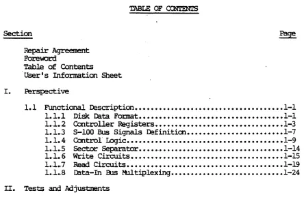
TABLE OF CCNl'ENI'S
Section
Repair Agreement
Fore~
Table of Contents
. User' s Information Sheet
I. Perspective
1.1 Furlctional IlescriptiOll •• , ••••••••••••••••••••••••••••••••••• 1-1
1.1.1 DiSk
Data Fo~t•••••••••••••••••••••••••••••••••••• l-l
1 •. 1 •. 2 Controller Registers •••••••••••••••••••••••••••••••• 1-3
1.1 •
.3S-IOO
Bus Signals I:'efiniticn ••••••••••••••••••••••••1-7
1.1. 4 Caltrol' I.ogic ••••••••••••••••••••••• " •••••••••••••••• 1-9
1 •. 1 •. 5 Sector Separa.tor ••••• ' ••••••••••••••••••••••••••••••• 1-14
l.l.6 Write Circuits •••••••••••••••••••••••••••••••••••••• 1-15
1 •. 1.~7 Read Circui'ts ••••••••••••••••••••••••••••••••••••••• 1-19
1 •. 1 •. 8 rata-In Bus M.lltiplexing •••••••••••••••••••••••••••• 1-24
II. Tests and Adjustm:mts
III.
2 •. 1- Con.t'roller. Adj'llStm:mts' ••••••••••• e" • • ' . ' . a·., • • • • • -• • . • . • • • • • • -• • • • • 2-1
2 •. 1.1 Test COnfigura.tiat •••••••••••••••••••••••••• -••• " ••••• 2-1
2.1.2 Center Frequency Adjust Test Procedure •••••••••••••• 2-1
2.1.3 2 us Single-Shot Adjust Test Procedure •••••••••••••• 2-1
2.1.4 1 us Single-Shot Adjust Test Procedure •••••••••••••• 2-1
2.1.5 Acceptable Liroits ••••••••••••••••••••••••••••••••••• 2-2
2.1.6 Adjustment Procedure •••••••••••••••••••••••••••••••• 2-2
Troubleshooting
3.1 3.2 3.3 3.4 3.5
Micropolis Disk Diagnostic ••••••••••••••••••••••••••••••••• 3-1 Voltage Measurements ••••••••••••••••••••••••••••••••••••••• 3-1
Checksum of the Bootstrap PROM's ••••••••••••••••••••••••••• 3-2
Read ~ratiOll ••••••••••••••••••••••••••••••••••••••••••••• 3-2
Write Operation •••••••••••••••••••••••••••••••••••••••••••• 3-3
Micropolis Disk Controller Board Technical Information Manual
I. PERSPECrIVE
1.1 Functional Description
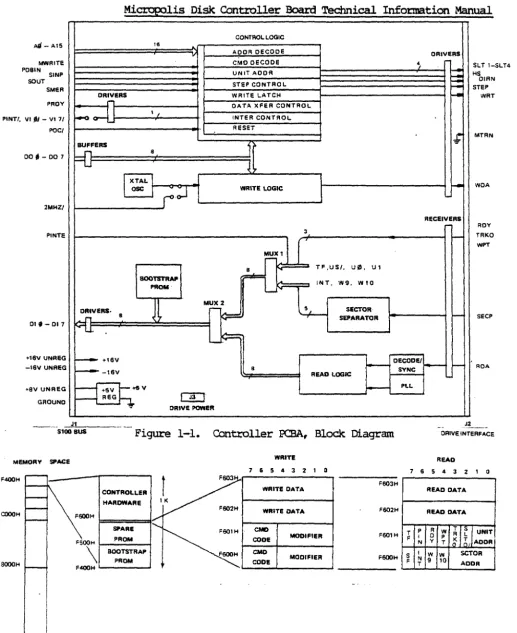
The Micropolis Disk Controller Board (Figure 1-1) is :i.mplemente:l al a
5-by-10 inch l?CBA that- plugs into the 5-100 bus. The controller contains
the followiIXJ major functional units:
a) Control logic to interpret CPU selection and respond to CPU
a:mnands.
b) A sector separator that separates sector and index pulses and keeps track of eadl sector as it passes under the read/write head.
c-l Write logic that converts parallel-form bytes fran the
au
to serial data suitable for- recorclin;J al the disk.d) Read log ic that converts the serial da ta from the disk to parallel-fom bytes for transfer to the CPU.
e) Bc:x:>tstrap PlD!s for z:eading sector zero of the system disk into RAM,
then startiIXJ the, ptOglatf in RAM.
l.l.-~ Disk Data. Format
Data is re.corded a l the disk in concentric tracks. The outernost track is track
zero..
Each track is divided into 16 sectors. The beginning of each sector is indicated by a sector hole punche:l in the disk. An index hole is located halfway between the holes for sector 15 and sector zero. The sector and the index hole are sense:l by a photo transistor in the diskdri ve. Each disk sector consists of a preanble, sync byte, header I data, a
checksum, arrl a postarnble. Eadl of these fields are describe:] below. Preamble
'!he preamble is canpos~ of approximately 40 bytes of zero (0) data bits. The preamble is automatically generated by the disk controller and is necessary to prov ide tolerana! for the nechanical aligrnnerit arrl electrical characteristics of the sector/index sensor. It also provides a field of known data pattem for synchronizaticn of the reed data decoder.
Sync Byte
The sync byte is a byte of data (FFH) which is used in the disk controller to define the beginning of useful data.
114-AI5 MWRITE P081H SINP SOUT SMER PROV
PINTI. VI.' - VI 71
POCI
2MHZ/
PINTE
01. - 017
"av UNREG -16V UN REG
.ev UNREG
GROUND
Micropolis Disk Controller Board Technical Infonnation Manual
CONTROL LOGIC
16
..
" AOOR OECOOE DRIVERS
CMO DECODE 4 SLT
1-UNIT AOOR
r::;
HS~
OIRN STEP CONTROLSTEP
DRIVERS WRITE LATCH
r-
WRT~O-U
I / DATA XFER CONTROLINTER CONTROL RESET
.;
MTRN BUFFERSi
fG
8{
X TALI- WOA
OSC
~ WRITE LOGIC
RECEIVERS ROV 3 TRKO t -WPT ~Xl
~
, TF.USI. uf/). UlBOOTSTRAP
.--- INT. W9. Wl0 PROM
L.-L
J~
MUX2ORIVERS·
C-rc=
SECTORN
8 SEPARATOR i- SECP"-~
f - - 'Iav
I - - OECODEJ I-- I
-! - - 1 6 V 8 SYNC
ROA READ LOGIC
~~v
I - - PLLREG
00·
DRIVE POWER
Jl J2
SI00 BUS Figure 1-1. Controller PCBA, Block Diagram ORIVE INTERFAce
MEMORY SPACE
F400H COOOH 8000H OOOOH CONTROLLER HARDWARE SPARE PROM BOOTSTRAP PROM
WRITE READ
7 6 5 4 3 2 I Q 7 6 5 4 3 2 1 a
F603H
WRITE DATA READ DATA
WRITE DATA F602H READ DATA
CMO
MODIFIER F60IH CODE
T P R
W ~
I
~J UNIT F I 0~ ~! b, AODR
N V
F600H CMO
CODE MODIFIER F600H
S I W W SCTOR F N 9 10
T AOOR
Micropolis Disk COntroller Board Technical Information Manual
Header
The header is a 2-byte block consistiDj of the binal:Y track address of
the track en which the sector res ides ( 0-76 ( 34 » and the address of the
sector (0-15). 'lhe header is used to verify that the proper sector is being
accessed in a disk. I/O operation.
rata.
The data field consists of 266 bytes of user data.
The checksum is a one byte error detection code that provures error
detection in read operations. The checksum is computed by the CPU as
follows:
a) '!he acClmlUlator and carry are initially cleared;
b) Each byte· of the header anJ data fields is added to the .accumulator
with carry.
In write operations, the computed checksum is written immediately
following the- data. field_ In read cp!rations, the checksum is recomputed
fran- the· read: data:
am.
is: caopared with the checksum byte which is read. Ifthey 00 oot o:::mpare, a. read- error has occurred •.
Postamble
The rest of the sect-or fran the checksum to the next sector hole is filled with zero data bits. The length of the postamble allows for the
mechanical tolerance in the placement of sector holes on the disk and
tolerance for disk speed and write clock variations.
1.1.2 Controller Registers
The controller is accessed usiDj the rnenDl:Y-mapped I/O technique; that
is, the controller a:mnand, stabls, and data registers are treated as JIeIIDry
addresses, so that the controller read/write ccmnands are actually memory
reference instructions. See figure 1-2 for a pictorial illustration of the
controller registel:S
am
the standam address configuratien.One. kilobyte of the CPU's memory space is allocated for use by the
controller. The upper 512 bytes are reserved for operatin; the controller
and the lower 512 bytes are allocated :fur the I::xJotstrap PRCMs. Because cnly
half of the available PROoi is used, only half of the lower space is USe:l.
The controller hardware registers Ot..oocupy the the first four locations of the
upper 512 bytes; and the remainder of the address space duplicates these four addresses over and cner.
Jumpers WI through W4 allow the controller to I::.e locatErl at aIr:! one of
Micropolis Disk Controller Board Technical Infornation Manual
the upper 16 lK blocks of CPU menory space (base crldresses COOOH to FeOOH).
The controller is normally configured with only jumper W4 installed,
selecting the IIeIIDry block starting, at FSOOH,
as
shown in figure 1-2. Thecontroller command, status,
am
data register:s are alS) indicated in thisfigure and are accessed by the appropriate CPU memory read and wri te CCI1IllaIlds.
Catmand r.:eqister
The command register, located at FAOOH or FAOlH far CPU
memory
writeoperations, provides for drive uni t/head selection, interrupt oontrol, write
enable, track-to-track stepping, and controller reset. The CPU sets the
oomnand code in bits 7, 6, 5 and sets the ItCdifier bits in
a
thru 4. Bitspecifications for t1:e C'Cl1Il1aI'rl register are sha.n below.
CCmnand Code
(bits 7,6,5)
o
1.
2.
3
4
5
6
7
Modifier
(bits 0-4)
Select DrivejHead {Bits 0,1: Select drive unit
address ( 0-3 )
(Bit 4: Select: head: O=lower~
l~r
Interrupt Control (Bi to: =0 Disable sector
interrupt
=1 Enable sector interrupt
Step 1 track (Bit 0: =0 Step out (decrease
track nurri:ler
=1 Step in (increase
track nurri:ler
Set WRITE Not used
Reset Controller ~t used
Not used Not used
Mic:ropolis Disk Controller Board Technical Information Manual
Sector Register
The sector register, located at FAOOH ~or CPU memory read operations,
contains the address of the sector currently passing under the reaq/write
head, and contains the sector fla;;
am
sector interrupt flag as they occur.'!be sector register forms controller status byte zero. Bit specifications
for the sector register am s.how1 below.
Bits lRfinition
0-3 Sector Address: Address of the sector passirg under the
mad/write head of the select drive.
4 Reserved: Jumper WIO
5 Host
au
Speed: .::J\.nrq;Jer W9 is installed according to mstCPU speed as follows:
1
=
~au
(W9 not installed)o
=
4MHz CPU (W9' installed)6 Sector Interrupt Flag: Indicates an interrupt request has teen
generaterl by a sector pulse. Fla;; is reset by issuirg a reset
or an interrupt disable camnand. (Not used by Micropolis
software.) •
7' Sector Flag: Indicates the sector address is valid and that
a read or write operaticn may I:e performed. Fla;; is true
for 30 usec at the start of each sector. All. data transfers
must I:e intiaterl within 100 usec of the flag goirg true.
Micropolis Disk Controller Board Technical Information Manual
Status Begister
'!he status register, locatErl at FAOm for CPU tnellOl:Y recrl operations contains
drive select and status bits, CPU interrupt status, and a flag t,obich enables the
CPU to synchronize disk read
am
write operations. '!he status register fonnscontroller status byte ate. Bit specifications for the status register are
shawn below.
Bits Il:!finition
0-1 Unit Address: Address of the currently selectErl drive. Address
~ is valid ooly if SLTD/ is true (0).
2 SLTD/: Unit selectErl • This flag is low true, ie.,
O=A drive is selected.
1=N:> dri w is selected.
SLDr/is true if a drive has l:::een selected and the 4-second tin'er has
not expired.. SLTD/is low t.rt.Ja 9:) that the software may detect when
the controller is oot installed (non-existant rrem:>ry references
yield OFFll).
3 TKO:. Track 0 status. fran selected drive·.
4- WPI":: Write: protectErl status fratt selectEd drive.
5 RDY:: Ready status fran the selected drive. When true, indicates
the dri Wo' is ready to perfOtIn ccmnands.
6 PINl'E:PINI'E status fran the 8-100 BUSS.
7 TF:Transfer flag. In write operations, indicates that the controller
is ready to accept data fran the cx:IIIFUter. In read cperations,
indicates that the controller has data available to the canputer.
When the software detects the transfer flag has set, all data
transfers are perfonned by access in; the controller data register,
Micropolis Disk Controller Board Technical Infornation Manual
Write rata Register
The write data register, located at FA02H/FA03H for a CPU memory write
operation, enables the CPU to write data on the disk. If the wri te da ta
register is referenca:3 when the transfer flcg is set durin;J a write operation,
the controller expect'S a data byte to l:e en the 8-100 bus data lines. The PRDY
line will be set true for 1 bit tine (4 usee). (See the'status register
descriptim for the definition of the transfer flag).
lead rata register
The read data register, located at FA02/FA03H for a CPU memory read
operatim, enables the CR1 to read disk data after it has been assembled into
parallel fom by the controller. If the reed data register is aecessErl when the
transfer flag is set during a read operation, the cxmtroller will hold the PRDY
line. false until a byte of data is available. The controller will then place
the data en the 5-100 bus lines and set the PRDY true for 1 bit time (4 usee).
The data will cnly be available for this 1 bit tine period.
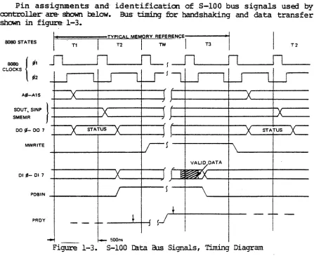
1 •. 1 .. 3 5-100 Bus Signals definition.
Pin ass'ignments and' identification of 5-100 bus signals used by the
controller- are· shown below. Bus' timing for handshaking and data transfer are
shown in figure- 1-3.
8080 STATES II
T1
TYPICAL MEMORY REFERENJ;E • I
T2
r
TWI
T3I
T2-
{.,
Ct.OCKS
~2
r-1l
n~__
~n~__ _
Af-A15
SOUT, SINP
I
SMEMR
DO st-007 STATUS
MWRITE
01 iI-01 7
POBIN
-f---+---J
PROY
Figure 1-3. 5-100 rata E\ls Signals, Timing Diagram
Micropolis Disk Controller Board Technical Information Manual
DISK CONTROLLER S·100 BUS INTERFACE
Signa' Pin Dim Descrfptlon Signal Pin Dlrn Description' Note
AOO 79· SINP 46 IN I/O Input Cycle
A01 80 SOUT 45 IN I/O Output Cycle
A02: 81 SMEMR 47 IN MEM Read .Cycle
A03 31 MWRITE 68 IN MEM Write Strobe
A04 30 PO BIN 78 IN CPU Data In Strobe
A05 29 PROY 72 OUT CPU Ready Line
A06 82 POCI 99 IN Poweron Clear
A07 83 IN Address
A08 84 Bus 2MHZI 49 IN 2.0 MHz Xtal Clock 4
A09 34
A10 37 PINTE 28 IN CPU INTELine 5
A11 87' PINTI 73 OUT CPU INTLine 5
A12 33
A-13 85, V101 4· 5
A14- 86 VHI 5 5
A15 32. V121 6 5
V131 7 OUT Vectored Interrupt 5
000 36 V141 8 Lines 5
001 35 V151 9 5
002:- 88: V161 10 5
o03~ 89< IN . oat8l0ut V111 1'1 5
004- 3S' B'us~
~OS' 39 GNo 50 IN Ground
006 40 GNO 100 IN Ground
007 90
+8V 1 IN +8V Unreg
010 95 +8V 51 IN +8VUnreg
011 94·
012 41 +16V 2 IN +16V Unreg 6
013 42 OUT Data In -16V 52 IN -16V Unreg
014 91 Bus
DIS 92
016 93
011 43
NOTES:
1. Slash (I) at end of signal name indicates Low True polarity.
2. All signal lines at TTL levels. Input lines require 1.0 mA max drive current Output lines driven by 74367 (32 mA sink).
3. Signal lines with notes are optional and are not used in the standard MicropoUs controller configuration. 4. Jumper option selects 2 MHz bus clock tor write circuits instead of Internal oscillator.
5. Jumper option generates interrupt on PINTI or V101 thru VHI on occurrence of each sector pulse. PINTE indicates current CPU interrupt status.
Micropolis Oisk- Controller Board Technical Information Manual
1.1.4 Control Logic
The control logic interprets the selection of the controller by the CPU
(Address decode), decodes the a::mnand byte to determine the selected drive unit
and to execute- the CPU ccmnands, controls data transfer b:!tween the drives and
the-
cro,
and generatesem
interrupt signals corresponding to sector pllses.Address JRcode (See sheet 2 of the schematic)
The_ address decode consists of decoder 08
am
its associated NAND gate andinverters. It m:::nitors: the c;ddress lines fran the
em
to interpret selection ofthe controller.
Whenever an ~ress is within- the lK block assigned to the controller, 08-9
will go low, and will be inverted by the C7-8 to form BSEL (boal:d select).
Also, the low at 08-9 will b:! gated at 06-10 with the inverse of A9 to £Om CSEL
(controller select)., CSEL is invertED by C7-4 to form CSEL/,
am
als:> I:e gatedwith Al to form r5EL (data select). When CSEL and MWRITE (memory write) are
high and A,l is low, C8-6 goes lOtI to for
OID/
(ccmnan:J code).Cam1and Iecode: (See: sheet_ 7 of the schematic)
Commands; are, decoded by- decoder 03 which examines the ccmnarxl llDdifier bits
fran the- CPU and generates the ccntroller a:mnand codes. 03 examines bi ts from
the CPU and generates the a:>ntroller- CCIlIllaI')j codes. D3 examines
CMD/
am
databits 05, 06, 07~ and generates me of five cx:mmands:
MJRC/
(address c:onnnand forselected drive),
INTC/
(interrupt ccmnand),STEPC/
(step ccmnand),WR1'C/
{writea:>nmand, and RSTC/ (reset o:::mnand).
Unit Address Cmtml (See sheet 8 of the schematic)
The unit address control consists of register B3 anj assorted NOR gates and
line drivers. It examines data lines fran the CPU, stores the selected drive
and head addresses, and generates drive
am
heal select signals for the driveinterface.
When RST/ (reset) is high
am
a drive unit select caIIlIa1'll is executed to fomADRC/,
B3 is clocked and stores the contents of 00, Dl ( dri ve address) and 04(head address). Sirnultaneoulsy B3-l0 is clockErl causing US (unit select) to
set. B4 decodes UO and U1 into four drive select signals which are then gated
wi th
us
by interface drivers BS. US remains set until it is cleared by a lowFer/
as the result of a four sea:>nd t.inYaout or an RSTC/ a:mmand. For a doublesided drive, B3-15 selects either the lower (0) or the upper (1) head.
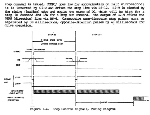
step Control (See sheet 8 of the schematic)
Step control is accanplishErl by flip-flcp B2 am its associated inverter C7-2
and line drivers B6-6 and B6-12. Figure 1-4 shows the circuit timing. When a
Micropolis Disk Controller Board Technical Infot:mation Manual
step cx:mnand is issued,
SI'El:C/
<.Pes low for approximately on half microsecond;it is inverted by C7-2 an:3 drives the step line via B6-l2. B2-9 is clocked by
the rising (leading) edge and copies the state of 00, Tt.tlich will be high for a
step in command and lew fat: a step out ccmnand. The outp.It of B2-9 drives the
DIBN (diJ:ection) line via 86-6. Consecutive. same-di:rection step pllses must be
separa,ted by 30 milliseCOl'lds'i opposite-diJ:ecticn pulses by 40 milliseoonds for
drive. ~ration.. '
STEPC/
011·
S2J9'
STEP IN
I-_>-;;'~ 30MS SAME- DIRN ~40MS CHANGE- DIRN
STEP OUT
u
{
I
Ir---_ _ _
_
DRIVe STEP·
4,
~
INF. DIRN-
~'I
i-lr-i---",g:g~~~ ~~
READ OR' WRITEOPERATION
Write Latch
I·
~ 40MS - - - -_ _ -1_,~
Figure 1-4. Step Control Signals, Timing Diagram
The write latch logic consists of flip-fle;> B2-5
am
its reset logic. When awrite ccmnand, is issued, WRrC/ goes low and the rising (trailing) edge sets
flip-flop B2-5., The WRT (write enable) outpIt at B2-5 enables the controller
write circuits and asserts the WR:r interface line via 136-6 (See sheet 6 of the
schematic). Writing occurs in the selected drive when WRr is true. B2-5 is
normally :reset by SP/ (sector fUlse) g::>ing low at the end of the sector; it will
Micropolis Disk Controller Board Technical Information Manual
Reset. Circuits (See sheet 7 of the schematic)
The reset circuit generates R5T/, the general reset signal for the
oontroller~ ']he circuit oonsists of a four-second me-shot 01-5 and associated logic ..
D~-5 is a t:etriggerable me-shot which is triggered by DIG/· each tine the
cm
reads fran the controller status or data registers. This occurs llloalW times a
secald \\!hen the OXltroller is in use causing D1-5 to remain high. If there is
00 disk activity for a perico of four seconds, 01-5 goes -10#1 causirg a 1011 RST/.
other- i.nplts to BST/ are RSTC/ (t:eset o:mmand) and RX: (5-100 power-on clear).
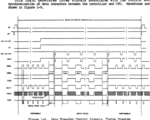
Data Transfer Control (See sheet 6 of the schematic)
This l.ogic generates: three signals associated with the control and
synclu:onizatioo of: data transfers between the oontroller and
cm.
Waveforms areshown' in figure. 1.-5.
SF
SPI
_________________
R_EA_O_O_R_W_RI_TE_O_~;A-T-IO-N---f---·~I~
f
- - - 5
r
WF OR RF J
.---1
TF f
---.J
, - - - f - - - f - - - - il
~
f--""'L
WPI OR RPI
0614
LrJ---u-t---U-I~
SSEL DSEL
05/8
05/11
PRDY
DIGI
PREAMBLE DATA FIELD POSTAMBLE
Figure 1-5.
cata
Transfer Control Signals, Timing DiagramMicrcpolis Oisk: Controller' Board Technical Information Manual
TF: Transfer Flag
This flag goes true one byte-tine before the first (sync) byte is to be
transferred to/fran the
cx:ntroller.
It is formed by gates 06-1 and 06-13 byor'iBJ
together' WF (write flag.) fran the write logic and RF (reed flag) fran theread logic:. 'IF is, sensed by the CEO by reading status byte 1.
I?Rm:' Processor Ready
This line connects to the CPU ready input. When PROY is low, the CPU
executes continues WAlT states, freezing program execution in the middle of the
current machine cycle. The address data out lines remain valid duriIl3 this
time.. 'nlis facility is used to synchronize the transfer of disk read or write
data, between the. CPU
am
contmller.The tri-state PRDY gate (09-13) is enabled by NUID IS-li, and when enabled,
gates the output of 05-8 onto the PRDY line. PRDY is enabled when the
controller is l:::eing' accessed (BSEL high) during' a rnE!ltDry reference instruction
(SINP and &m' both low).
05-8 is; oot:maU.y high except r,.,hen the read or write data register is being
accessed; (USE[;. high)" 'IF' is high (data area of the· sector),
am
WP/ and RP/ areboth high- (controller not ready to accept. a byte of write data, or has not
assembled a complete byte· of. reed data). When the controller is reajy for the
transfer,. WP/ or RP/ SPes low for me-bit time· allowing the software loop to
proceed.
DIG/: Jl:lta In
Gate:-This signal gates controller'status, reed data, or P.RQ1 infoonatim onto the
5-100 bus data in lines 010 thru 017 (See sheet 5 of the schematic). DIG/
(C8-8) goes lCM when the controller is addressed (BSEL high) duriIl3 memor:y read
Micropolis Disk Controller Board Technical Information Manual
Interrupt Control (See sheet 7 of the schematic)
When enabled, the interrupt control logic generates an interrupt as the
sector flag' (SF) <.J)es high at each sector I::x>\mdary. Figure 1-6 illustrates the
timing of this'· circuit.- The. interrupt may be jumpered to PINT/ (processor
inten:upt.) or ale of the vectored interrupt lines VIO/ thru V17/. The logic
consists of interrupt
enable
flip-flop 02-5, interrupt flip-flop 02~9,and
thedriver 010-13.
SECTOR BOUNDARY CLEAR INTERRUPT
/
/ABLE ~RE-ENA8LE
-~~
: \
II
1,-=--
_.
INTCJ
INTEN (02/5 I
LJ
S F·
I
INT (0219 II
I
PINT/. VI 'I-VI 71
I
I INT. SERVICE ROUTINE--- --- - ---- --_._-' . , ____ 1. _ L ______
-NOTE: INTERRUPTS ARE' NOT ~ WITH_MICROPOLIS SOFTWARE _ _ _ _ _ _ _
Figure 1.-6.. Interrupt Signals, Timing Diagram
When an interrupt control command is issued, 02-5 is either set or reset
depending on the state of the IlCdifier bit ~O. When set, interrupts are enabled
allowing 02-9 (IN!') to set at the 'followirg sector boundary (risirg ed~ of SF).
'lbe resulting low at 010-13 drives the desired 5-100 interrupt line by means of
a jumper connection. '!be interrupt is cleara:3 by the interrupt service routine
by issuing another interrupt a:>ntrol cxmnand with DO=O.
'!be interrupt logic is initially cleara:3 by RST/ low.
/
Micropolis Disk Controller Board Technical InfODnation Manual
1.1.5 Sector Separator (See sheet 6' of the schematic)
SEep'
C2/13
e2/s
ROS
WOS-SF·
SP/
sill
St
52
S3
The sector separator uses SEeP (the drive sector hole photosense outplt
received at 87-4-) to generate the' sector timing signals
:ros
(read ooe-shot) andits. compliment ROS/,- was/ (write- one-shot), SF (sec.tor flag), SP/ (sector
pulse), and SO thru S3 (sector eot.mt signals). It oonsists of one-shots C2, Cl,
and 013, and four-bit· counterC3. Figure 1-7 illustrates the timin; of this
circuit.
1 - - - 1 ReVOLUTION
---l,1
200 MS
I I I
r
-n-
700USn
n
~
.J1
n
I I I
~200US
[1'
n-
n
~"
I I
n
-fl-JOUSn
r"
L;.;-lJ
n
r"
I I I
+
IUS Uu.
nr r-u
u
u
I I I
~
II
I
I
G
I
I
I
I I
I
i
~
r-1
I
II
I(
I
>
I
Figure 1-1'. Sector Separator Signals, Timing Diagram
rL-
fL-
ur
-ROS is generated as follows: one-shot C2-13 shapes the leadin; edge of SECP
into a me-micrasecond I;Ul.se \>hich is used by one-shot C2-S to form a pulse of
approx·imatel.y three quarters of a second period; the pulse bridges the tine
during which the index I;Ul.se occurs. '!he pllse at C2-S triggers one-shot Cl-13,
which forms a 700 microsecond ROS period to provide time for PLL and read
logic-decode circuits to synchronize before a sector is read. C2-S also
triggers one-shot Cl-5 which generates a 1200 llS t:ine pericrl durin; whim the
Micropolis Disk Controller Board Technical Information Manual
SF is a 3Q-microsecond pllse formed \\hen me-shot 01-13 is triggered by the
leading edge of the C2~5 pulse:
The
high focne:3 at 01-13 is delaye:3 through ANDgate C6-3 by Ie network c:7 and R13 to form SF. This delay (approximately 200
ns) ensures that the sector oounter
is
stable at the new sector address when theCPU senses SF true.
5P/ consists of a one-microseoooo 1cM trt:e pulse for eadl of the 16 sector
holes in the diske.tte. Each pulse defines the end of one' sector and the
beg inning of the next.. N:> pulse is generated for the index hole. It is fonned
by gating C2-13 with C2-l2.
SO thru 53 are the outpu.ts of a 4-bit counter C3, whim is incremented at
each sector tX>lmdary. 'nlese lines indicate the binary address (O-ls) of the
sector currently under the read/write head. '1tle counter is synchronize:3 with
index by loading a oount of 15 when the index tDle is sensed. SF
am
SO thru 53are sample:3 simultaneously by the CPU by readirg status byte O.
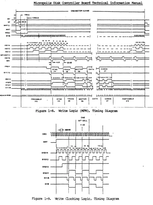
1.1.6 Write Circuits; (See sheet. 3 of the schematic)
The write circu.its accept. parallel data bytes 000 thru 007 fran the CPU via
09 and 010.. 'nle data is serialized then decoded into MFM form to generate WI:ll\
(w·rite data!).. '!his signal is route:3 to the select drive via B6-l0 (See sheet 8
of: the. schematic:) _ 'nlis. logic consists of the write bit and byte counters,
shift register,. encodirg' the. pulse shaping circuits.
_Write timing is. derived fran a 2 MHz
esc
(oscillator) signal from a crystaloscillator (See: sheet 7 of the schematic). An alternate 2 MHz signal may be
obtained from the. 5-100 data bJs via Jl-49 if jUIIlJ;er Wl2 is installed.
The write logic is normally configure:3 for MFM encoding: J:buble frequency
encoding can be used in place of MFM if jumpers W6 and W7 are removed and
jumpers WS
am
W8 are installed. 'Jbe Micropolis software is configuroo for MFMoperation ally. Figures 1-8 and 1-9 provide timing information on ther write
circuits. Write timirg is derived fran a 2 MHz OSC/ (oscillator) signal fran a
crystal oscillator (See sheet 7 of the schematic). An al ternate 2 MHz signal
may be obtained fran the. 5-100 data bus via Jl-49 if jumper W12 is installoo and
Wll. is anitted.
Micropo1is Disk Controller Board Technical Infonnation Manual
A9114
A9/13 A9/12
WFtA911U
A9115 WPI
ONE SECTOR 12.5 MS
~---I f
-J 10 " . . 9 11 13 15 9
~~
. . ' . ."':~;
. . . " . :t~
- . : : : ._-=-=j
---I-j~---j
=
-;;~;~
,
n~
U~
PROY _ _ _ + ________ ...,.
=1-~ 4US
1-
nus:r-l=================;~
~---J ~
_ _ _ _ IJ'UlJtJ'IJlJtlt,
-a 910 "12,
1- _ _ _ _ _ _ _ _ _ I-J"U'1J'1..I1...
l - - - ----J-~
l---~I-~
I I i
~ nU nU
I,
I SYNC ITRACK tsECTOR I DATA
811:12 _ _ _ +-_ t FF T 3E t 05 t
89113
---,1 ...
~,..
..
£
A10/5 _ _ --IrT"
:=====:t! ';,-
;;~~
013/1
===1=
A11/8
WOAtAtO/91 _ _ _ ..f-L...a....J..II..II..II..JI..JluIUIUIL..IL.Iu..1 1..1 1..1 1..1 1..1 .l,.1...&...IL.IL.1u..1 1...1 1...1 1..1 ..11...1..1 1...1 1...1 1..1 .l,.1..J1..J1L..IL.1u..1 ..II-..II...II~
PRE-AMBLE-a's SYNC FF
I
TRACK nI
SECTOR-05j I 1 I I I I 1 1 II I 1 I " II I I j...u..JI..JI..JL..I..JL..l4-_
CHECK
I
POSTAM8LE 21 O'S OATA. .
-Figure
1-8..
Write Iogic (MFM), Timing DiagramaSCI
WRT
810/14
810/13
810112
S10/11
81116
8718
ONE
81T CELL 4 US
Micropolis Disk Controller Board Technical Infot:mation Manual
The following sequence of events occurs when a sector is written onto the diskette:
a. '!he disk I/O driver B):etware selects the required drive and IlDves the
positioner to the desired track using DRIVE SELECl' and Sl'EP cannands to the
oontl:Ol1et: ..
b. The dt:iver continually reads status byte 0 look:i.n;J for SF trt.:E with the
desired sector aJdress.
c. When the desired sector is found, a SEt' WRITE cc:.mnarrl must tE issued
within 70 us (i.e., within 100 us of the physical beginning of the sector).
'!his sets the· WRr flip-flcp in the oontroller causin; the preamble to tE written
onto the diskette.
d. The driver continually reads. status byte 1 1ook:i.n;J for the TF (transfer
flag:) true. ']his, 0CCUl:S at the end of the preamble when the sync byte is about
to be. written.
e. '!he driver must wri.te the sync byte pattern (FFH) to the write data
register within 20 us after detecting TF true. The controller responds by
pulling the. PRDY line· .low thus lDlding the sync pattern on the DATA OUT lines
until. it is' ready" to;· accept the byte .•.
f. Q1e.-byte time:: (32. us;) after TF" goes tme·,. the controller copies the synch
byte into the. write: register
am
raises. the PRDY line allowin; executiO'l of thesoftware loop to proceed.
g. rw:in;J the follCMin; byte-tine, the sync byte is serialized, encx:lded, and
written O'lto the disk. At the same tine, the driver accesses the following byte
(cylinder address), computes a partial sumcheck,
am
writes the byte to thewrite data register causing PRDY to g:J low again.
h. Steps f and g are repeated for eadl byte of the header
am
data fields.'!he sumcheck byte. is then written imnediately after the last data byte.
i. The: contt:oller automatically fills· the remainder of the sector with an
all-zeroes pattern. When. the following sector pulse is encountered, WRT is
autanatically' reset in the. controller endin; the write operatiO'l.
Write Bit Counter (See sheet 3 of the schematic)
'!he write bit. counter consists of oounter BIO and NAND gates B7-8
am
Bll-6.'!he WRr signal. fran the write latch enables bit oounter BIO and the remainder
of the write circuits. BIO then oounts the 2 MHz
asC/
pulses and produces thewaveforms
slx:>wn
in figure 1-9. Oltput B10-11 (OSC divided by eight) cxnsists ofa square wave with a period of one bit-tine (4 us). This is invertaJ by B7-8
and used to clock the byte counter A9, and data shift register 89. NAND gate
Bll-6 decodes a count of 7 or 15 in BI0 causin3' a count of 12 or 4 to l::e loaded
into the counter.
Mic;opolis Disk Controller Board Technical Information Manual
Byte Counter (See sheet 3 of the schematic)
The byte counter' consists of A9, flip-flcp B12-S, an:] inverter 014-4. '!be byte. COtmter counts off ccnsecutive groups of 8 bits which correspond to each byte of data recorded on the: diskette. '!he signal
WP/
(write pulse) goes lowfo:c' ale- bit-time: at the. beginning of eaCh byte •.
Counter A9 is inhibite3 by
was!
lew while the preamble is bein;r written (Seefigure ~-7). After approximately 1200 us,
waS/
~es high allowing . A9 to bec~ocked by the rising edge of each bit-tine pulse fran B7-8. A9 counts off consecutive bits of data LIlti~ it reaches the count of eight: at that time, WF
(write flag) goes high indicatin:J that the
sync
byte is about tore
written. A9 then continues oounting until 15 is reached, at 'lbich tin'e A9-15 (carry ou tpu t) goes' high causing A9 to load a count of eight, and then to contim.e in thesequence 8-B, 8-15, etc·. E'ach 15 count (M-15 high) corresponds to the last
bit or a. byte·.. This signal is delayed by B12-5 to form
wP/
which goes low during the following: bit-time...WP/
low causes PRDY to cp high for 4 us,allowin:r the software loc:p to. proceed •.
Shif.t legister (See sheet 3 of the· schematic)
The-- shift l:e.<Jister logic:. cons:ists: of' a. paraileJ..:-to-serial. register B9 and
NAND' gate: Bll-l2.., 'lhe· shift register.- converts the para.lle~ 000 thru- 007 data
inputs: to: serial. data output at pin 13, as sham in figure 1-8 •.
Illring the last bit of: each byte, A9-l5 high causes Bll-12 to g::J low pt'ovided that the. CPU is writing to the write register address (ll5EL an:] MWRITE both high).. 'nlis places the shift register in load node causing the contents of 000 thru 007 to be copied into the register on the following clock. This infonnation is shifted right and appears at B9-l3 in serial form during the fOllowID; byte-tine.
After the sundleck has teen written, the software nakes no further reference to the. write register and the register is not loaded. A continuous strean of zer:oes entering at B9-~ is shifted through the register to form the p::>stamble pattern.
E'ncoding and Pulse Shaping' Circttits (See sheet 3 of the schematic)
The. encodin.:r circuit consists of AlD-S,. 013-1, and All-6. The pulse shaping circuit ccnsists of 013-4 and AID-9. 'lhese .circuits encode and shape the data stream fran B9-13 to fom WDA •
. '!be rules for MFM (double density) and OF (single density) encoding are usually state3 as follows:
Micropolis Disk Controller Board Technical Information Manual
Rule 2 MFM: A flux transition is t:ecOrded at the b:ginning of a cell if the
current
am
preceedi1'X.:J data bits 'are botho.
IF: A flux transition is recorded at the b:ginning of every cell.
rn
this implementation of the logic, rule 2 has IIDdifiei to an equivalent:furm: as~ follows:~
Rule. 2A MFM: A flux transition is recorded at the end of a cell if the
current and subsequent data bits are tx>th O.
OF: A flux. transiticn is recordErl at the
em
of every cell.Serial data from B9-13 is first delayed one bit-time by AIO-5. This
fl.ip-flop contains the data bit currently bein;; encoded. . D13-1 and All-6 then
. perform the encoding fimction as described above, where gate inputs All-4/5
introduce the data tou"'lsitions (Rule 2A). Output All-6 goes low for half a
bit--time for each transiticn to
te
recorded.013,-4, and A·l.0-9 shape this signal to fom
wm
which consists of a 0.5 ushigh-tJ:ue pllse for each transitioo. Line driver B6-10 transmits
wm
to theselected. drive .•.
1...1_7 Read.. Circu.its: (see: sheets: 4, and 9· of the schematic)
The following sequence. of events take place when a sector is rea:l fran the
disk::
a..
The disk I/O driver' software selects the required drive an:]moves
thepositioner to the desired track using DRIVE SELECT and STEP conunands to the
controller.
b. 'Ihe driver CDl'ltinually reads status byte 0 looking for SF true with the desired sector address __
c.
When the desired sector is fiound, the driver continually reads statusbyte 1 looking for TF' (transfer flag) true. This occurs <n! byte-tiIre before
the first. (sync) byte of. the sector is available to transfer to the CPU. Note
that no expl.icit Sgr READ command is required since the controller is always
attempting to read when it is oot writing.
d.. The: driver must attempt to read this byte fran the rea:l data register
within 20 us after detecting TF tJ::ue. '!he controller responds by pIlling PRDY
lcY.<I until
.
the byte is fully assembled •e. When the byte is assembled, PRDY goes high for ene· bit-tine allowing the
transfer to be canpleted. The driver must nO\1 process the sync byte an:] attempt
to access the following byte (cylinder address) in less than one byte-time. This causes PRDY to g::J low again.
f. Step e is repeated for each byte of the header, data, and sum::heck fields.
Micropolis Disk Controller Board Technical Information Manual
'!he driver re<::aDI;Xltes the st.md:leck frcm the header and data fields and compares
this against the sumcheck. reCMf fran the disk. A discrepancy indicates a disk
data transfer' error.
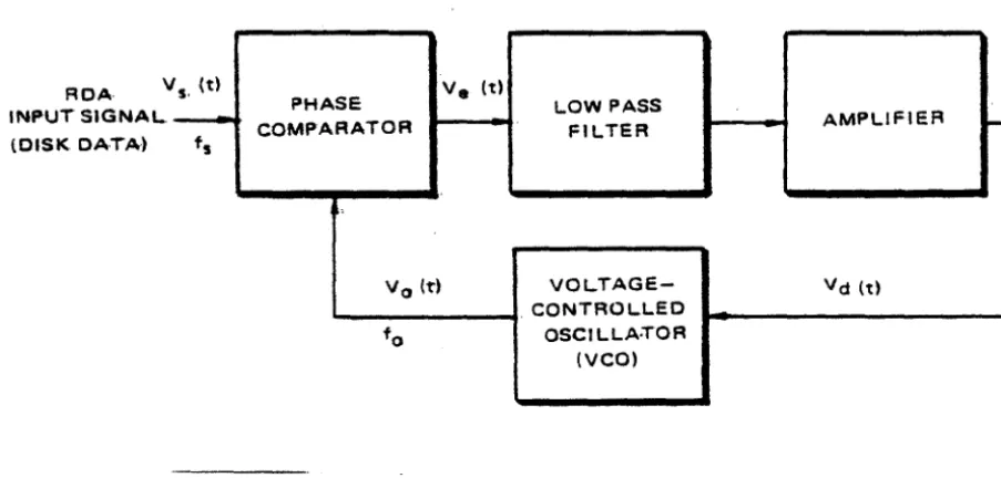
The. read, electronics' consists' of' phase-locked loop circuit (PLL), data
decoder', c:lock synchl::oniza.tion. circui.t,. seria~ -to-paralle~ converter, and
contml logic~.
PLL (See sheet 9 of the-schematic)
The purpose of. the PLL is to provide a clock signal for decx:xliIl1 purposes
which naintains a fixed
tilase
relationship with the ineaning read data signal,RDA. The. ELL is a feedback systE!\t consistin; of a phase canparator, a low-pass
filter, eo:or amplifier,. and a ~ltage.: controller cscillator (VCO).
A. block: diagram is· shown in figure 1-10 with m input signal applied, the
error voltage: is. zero and the ~ oscillates at its center frequency fu. ~en an
input signal. is: applied,. tba phase canparator.· o::mpares the phase
am
frequencyof the inplt with. the
vee
output, and generates an error ~l tage Ve ( t) that isre.lated to the difference- of. the 0.0 signals. This error voltage is filtered,
amplified." and routed: to the control. input of: the
vco.
'!hus the oontrol voltageVd.( t) fOrces the: \CO. frequency. to vcu:y in· a. dimctim that reduces the frequency
diffet:ence: between: fo~ and the- input signa!... If the· inpu.t signal. fs is
sufficiently close-- to; fo,. the: feedback. natUI.'e:· of the PLL causes the
vro
to lockwith: the- inc::aniIlg7 signal.. When locked, the-VCO frequency is identical to the
inplt signal." except. for a small. phase difference which is necessaq to generate
the correctioo signal which maintains the VCO at. the input data frequency fs.
m
this· way, the· PLL. can track variations in the disk speed, generatin:;J acontinuous clock. having a fixed
Fhase·
relationship with the incoming data, andwhich can l:::e used to decode the data pattem.
v
RDA INPUT SIGNAL.. (DISK DATA)
s. (t)
ts
PHASE COMPARATOR
Vo (t')
fo
V. (t)
LOW PASS
FIL TER AMPLIFIER
VOL..TAGE- Vd (t)
. CONTROLLED OSCILLA·TOR
(VCO)
Figure 1-10. Phase IDcked Ioop (PLL), Block Diagram
i-Micropolis. Disk Controller Board Tedmical Information Manual
RDA
RDOSIM4J13)
A,14/5
{
8,14,/8 (INC.)
8,14/6 IDE.C.)
CORRECTION SIGNA'LS
OSC (A15/7)
Cl'4/3:
PCLt<: (C14/2
C14/5
~ CELL WINDOW
DISCRIMINATOR CHARACTERISTIC
LJ
I
!=2US
LJ
I
I
n
I
OEtODERI I
I.
LJ
I
I
n
SAMPLES
,
I
I
Figm:e 1-11. PLL Circuits (MFM), Timing Diagram
Micropo1is Disk contz:oller Board Technical Information Manual
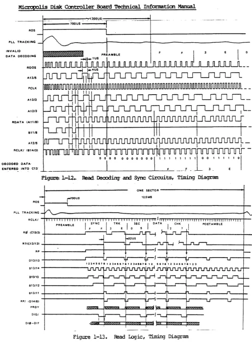
Figw:e 1-11 illustrates the timing of the PLL circuits. RDA is received at
B7;...10 (See sheet 8 of the sdlematic) an:] applied to one-shct Al4-5 to prodUCE a
2. us; p.Ilse for each flux transitioo read from the disk. The ene-shot output
connects to a phase comparator consisting of flip-flc:p CI4-5 and NAND gates
B~4:....li, -8,
and.
-6.. '!he. \U) oscillates at four' times the data rate, and itsoutput A15-7 is. first divided .. by two by Cl4-3 before c~ tlJe ccmparatcr
flip-flop Cl4-5.. Jumper W1A and W16-
are
installed for MFM qJeration or WI3 and.WIS" are installEd for IF op:!ratioo.. The PLL timin:J diagrcm fOr MEM is stx:>wn in
figure l-li ..
Corz:ectioo signals generated by' Bl4-8 and Bl4-6 are applied to a balanced low
pass- filter formed by R30, R32, and C1.7 on ale leg and R3l, R33, and CIS on the
other leg. 'llle filter output. is amplified by differential amplifier B15, which
in turn drives the cx:ntJ:o~ input to the
vco.
'!he CEnter frequency is adjustedby potentianeter R40,. and should' l:e set, at 1 .. 0 MHz for MFM (0.5 MHz for IF with
no data input).
Another one-shot ll4-5 (RIXS)" delays the leadin.; edge of each Rm pulse by
1.0 us l:efore: input to the::read decoding' logic: (See sheet 4 of the schematic).
When the PLL. is locked,- the fallin;r edge: of. each 1?CLK pulse occm:s at the center
of the, decoder ha~f-cell "'windows·n Le •. , midway between the times at which
potential flux: transi.ti.ons: occur. One.-shot. Al4-5 is adjustable allowing teLK to
bE!! moved wi.t±t respect to the: decoding' window-.. This provides a means of
optimirinq the w,indQW.i ad~ustment:
am,
of measurin.;- the read p:!rfOt'IllaIlC2. of thedri~ in: terms. of ert:Ot::-fr:ee; range of' adjustnent.. The, delay should be set to
1..0 us: for notmal. operatioo' •.
Read Data Ilacoder (See: sheet 4: of. the: schematic:)
The decoder consists of flip-flops AI3-5, AI3-3, A12-3, AND/OR inverter
All-a.. Using the i.np.Its RIDS and :t=CLK fran the PLL, this circuit decodes the
read data and gene·rates a high output for half a cell-tine at ~ for each
flux transiticn read fran- the· disk.. Timing for the. read data decode circuit is
shown in figure 1-12 ..
The· falling' edge of each
m:os
pllse toggles A13-5 as shown in figure 1-12.This output is a replica of the flux pattern as it is recorded at the disk.
EeLK' on Al3-l2 now samples the: rutput fran A13-5 at the center of each half-cell
window causing A13-3 to set. or' reset accordingly. A13-3 is then delayed one
half-cell by Al2-3. AND/OR inverter All-8 is connected as exclusive OR and
detects any change: of state at A13-3. 'llle outplt, RDATA, goes high for half a
Mic;oeolis Disk Cootroller BoaJ:d Technical Infonnation Manual
ROS
PLL TRACKING
INVALID
DATA DECODING
RDOS
Al3/S
PCLK
At3/3
At213
RDATA
811/8
A12/S
RCLKI (814/31
OEoCOOEO DA'iA-EN'fE-REoD
ROS
PLL TRACKING RCLKI
RIt (C13/31
R7(Ct3113) RI'-013113
813114
813113
B13112 B13111
RPI (014/6)
PRDY DIGI Dle-DI7
7 0 0 U S - - - -....
F'i:gure L-U.. Reac!. tecodin;' and Sync. Circuits, Timing Diagram
ONE SECTOR
---...!
~OOUS 12.5M8
PREAMBLE
Figure 1-13. Iead IDg ie, Timing Diagram
Micropolis. Disk Controller Board Technical Information Manual
Read Clock Synchronization (See sheet 4 of the schematic)
The circuit consisti.rg of Bll-8, AU-5,
am
B14-3 generates a clock signal,lCLK,. for the data transitiO'lS cnly which is used to sample the decoding read
d·ata.. This circuit IlIlSt b!. initially syn~izEd duriIl3 the preamble s:> that
, the correct (data.) half-oell is selected.,
Flip-flop A12-5 is' clocked by PCLK causirg the outplt tIl change state for
each half-cell that NMD output Bll-8 is high. A clock pulse is generated on
RCLKI when A12-5 is high as shown in figure 1-12. In the preamble area that
data pattern is known to b! all zeroes: Le.,
no
transitions should I:::e detectedin the data half-celL. During the first 700 us of preamble (OCS high), B11-8
tests. for this condition and the Oltput gJes low for cne half-cell if a one-bit
is detected.. '!his inhibits· AU-5 fran changirg state ore tine causirg the other
half:..eell
to
b! selected.. NXe the t;:eriod of IDS is long enough to cover bothsector-hole tolerancing' and. the PLL lockup tine. r:uriIl3 the remainder of the
sec.tor Bll-8 remains high. and RCLK/ pulses are generated during every
half-cell. ..
Read: Shift t:egister and Ccntxol. Iogic (See sheet. 4· of the schematic)
Shi£t. O!gister CD· assembles the decoded: data:: into byte-parallel fom for
transmissicn~ to the CBJ.,. '!he control. logic. CXXlSisting: of BU-9, 013-3, B13, and
D"l.4;-6i generates~ two control. signals,. RF and
RP/,
which coordinate the transferof each, byte.. See figures 1-12. and 1-13.
CD and B12-9· are initially held reset durirg the beginniIl3 of each sector by
ROSI
low.. WhenROSI
SPes high, zero bits are entered into the register lIDtilthe first bit of the sync byte :is encountered. At this tine, C13-3 goes high
and the rising edge clocks B12-9, causing RF to set. RF true causes TF
(transfer flag) tIl g:J true, signifyin; the the first, (sync) byte is alIrost ready
to transfer.
Counter B13 is intially preset to a count of
one
by a lew ouq:uton
D13-13.When RF goes true, the preset condition is reIn:)ved and the counter counts off
consecuti ve- groups of· eight bits correspondiIl3 tIl each byte. A fully assembled
byte. is: available· in the shift register when a' count of eight is reached. At
this tine·, the high outplt at 813-11 is delayed by 200 us, then inverted tIl fom
RP/.
RPI
low forces· PRDY high allowing the CPU to complete execution of thecurrent. instructim (real fran real data register). 813-11 high als:> produces a
low en D13-13, causing the counter tIl l:e preset tIl cne again at the teginning of
the· following byte.. '!be remaini.n; bytes of the sector are transferred in this
manner •.
1.1.8 Data In Bus Multiplexing (See sheet 5 of the schematic)
Micropc?lis Disk Controller Board Technical Info:r:mation Manual
The ~ C9 and
CIa
contain a bootstrap program which loads the systemsoftware from disk into memory after power-on. The bootstrap is enterErl by
transferring control to the controller base address (normally F8a aH) • A
description and listing of this program is given in paragraph 6.7 of the
Micropolis User I s Manual.
Signals cc:mprisin; status. bytes
a
and 1 arrl the reaj register outputs RO thruR7 are- Illll.tiplexed together by C4, CS, Cll, and CU. Status byte 0 is selected
if Al.AO
=
00; status byte 1 if Al.AO=
01;am
the reaj register is selecterl ifAl
=
1. The tri-state ootputs fran either the PIO-1s or Cll, C12 are enabled byCSEL or CSEL/ dependin] en whether the 10"Ner or upper half of the lK controller
address space is teing accessed. The selected byte is gated cnto data-in lines
DIO thru D17, by 011 and 012 when OIW is low.
Micropolis Disk Controller Board Technical. Information Manual
II. TESTS AND AO.:1t15'D1ENrS
2.1
ControllerAdjustments•
Controller adjustments consist of:.
a. Center frequency a3just.
b. 2 us single-shot adjust.
c. 1 us single-shot a3just.
2.l •. ~ Test Configuration
a. Inse.rt the controller in an 5-100 bus 8080/Z80 baseJ canputer using
an extender cam •.
b.. Connect. controller to aI'¥ Micropolis storage ItCdule.
2.,1 .. 2
center:
Ft:equency Adjust Test Procedure.a.. Ensm.e: that the driVla' is' not: on' ..
b.. COnnect oscilloscope to the· oscillator output at A1S-7. Set
oscillosoopa tine. base to 200
nsl
an.-c. Measure frequency of oscillator.
2.1. 3 2 us Single-Shot Adjust Test Procedure
a. Insert a diskette in drive.
b. B:lsition the head to track 0 and write a full track of 'ones' data
(16 sectors).
c... Eerform a: exntinuous read operation en track zero.
d.. Altemately select program Xl4 to achieve step; b an:l c.
e.. Connect cscilloscopa to A14-S, set time
tase
of oscilloscope to 200ns/en,.
am
observe
one-shot output.,2.1 •. 4 1 us Single-Shot Adjust Test Procedure
a. Proce€rl with step; a thru d, para. 2.1.3.
b. Connect cscillosoop:! to Al4-3, set time
tase
of oscilloscope to 200Microp:>lis Disk Controller Board Technical Infonnation Manual
2 •. 1.5 Acceptable Limits
a. Center frequency: 970 kHz miniImmt - 1033 kHz maximum.
b. 2 us single-sOOt: 1.94 us minimmn - 2.06 us ~imum •
.
c.. 1. us', smgie-shot:: 0 •. 97 us mininumt - 1 .. 03 us maximum.
2.,1 •. 6 Adjustnent Procedure
a. Center frequency: Adjust R40 until the output frequency is 1 MHz.
b_ 2. us single-shot.: Adjust R27 foz: a feriod of 2 us.
C'. 1 us single-shot: Adjust R46 for a period of 1 us.
Micropolis Disk Controller Board Technical Information Manual
III. Troubleshooting
3.1 Visual. Inspection
Visually inspect the disk: contl:Oller board as follows:
a. Cleek for evidence of blmt or damaged cx:t'I1{;X)nents.
b. Cleek for proper orientatial of polarized capacitors.
c. Fnsure pt'Op!r orientation of all jllIllt=er selected options (See
User I s Infot:maticn Sheet for details).
3.2 Voltage· Measm:enent
Connect the controller to a test systan
am
apply power. Measut:e thesupply voltages as follows':
a.. +5 vol.ts at pin 3 of VR-l.. +5 volts
+
5%.be.. -5 voi.t:s; at pin~ 4- of &-15. -5 volts.
+
5% •.c. +5 vol.ts: fil.tered at pin 7 of 3-15.. +5 volts + 5% with less than 10
millivol.ts of riwle..
-Should any of- these voltages b:! rut of tolerance, refer to the following schematic drawings for locatim.
a. +5 volts, page 8 of schematic.
b.. -5 volts, page 9 of schematic.
c.· +5 volts filtered, page 8 of schematic.
3.3 Checksmn of Bc:x>tstrap PBCM' s
A. checksum of the Bootstrap PROM's can be accomplished by using the
system l1IJ11itor's Q corranand followed by FSOO FSFF for standard systems.
Refer to User's Information Sheet at the beginning of this manual for
further information en the
teard'
s we crldress.The checksun of the Bc:x>tstrap PR:M's is BOl. Should a number other than
Mic;opolis Disk Controller Board Technical Information Manual
3.4 Read Operation.
To pet:form a read operation, insert an MOOS diskette with nDIAG" and
attenpt: to bJot up.. I f the. diskette cDes lDt boot, perform the following
check:::
a-.. Cleek fOr proper drive selection by checking pin 3 of B-5. Refer to
sheet 8 of the schematic. Cleek all signals en the schematic that relate to
the. read operaticn.
b.. Cleek fer. an indicatien of ~ at pin 10 of B-7. Refer to sheet 8 of
the schematic •.
c.. Check for the presense of SECP (Sector pulse) at pin 4 of B-7.
Refer to page: 8 of the schematic •.
d.. Check for the. proper binary countiIXJ of SO, 51, 52, and 53 at the
appropriate· pins, of C-3. Refer' to page 6 of the schematic.
e.. Oleck: for proper pulse widths fran the llDllOStab.le multivibratoI:S C-1,
C-2,
am..
o-l.. Refer to sheet 6 of. the: schematic.E_ Qieek: fOr: ~ pt:eSena!- of IcrJ{ at pin 3 of B-14. Refer to sheet 9 of:
the: schenati c-.
g. Check. for the presence' of ~ at pin 8 of A-1L Refer to sheet 4
of the schematic •.
h. Oleck for the presence of RCLK at pin 3 of B-14. Refer to sheet 4 of
the the schematic.
i.. Cheek: for the proper operatien of "data an:l status" mul tiplexeI:S C4,
CS, Cll, and CU. Refer' to sheet 5 of the schematic.
j •. Check for the presense of DIG at pin 8 of C-8. Refer to sheet 6 of the' schematic.
k. Ensure proper operation of the output data buffers Dll and D12.
Refer to sheet 5 of the ..
3.5 Write Operation
To perform a w·rite operaticn, insert an MOOS diskette with DIAG in the
proper drive and tx:x>t up. call up DIAG to the rrcni tor and you will see
ME'M DIA(3)5TIC VS 4.0
800031 REV A
en the screen.
Micropolis Disk Controller Board Technical Information Manual
Respald to DIAG as follows:
!IOff. B\NEL (Y CR N)?N
ENrER. BIGi 'mACK 76
~ a:::nmND Z",0,.0,.I,2
'!he a.bove a:mnan:l will. initialize, the drive to track 0
am
~ite a binarypr:oJ:ressioo al al~ sectors of al~ tracks.
ENrER ClltJMAND RD, 2
'Ibis CCI1I1laIrl will attempt: to real the pattem written by the ccmnand I,2.
My errors will be displayed al the screen. See Micropolis Manual, Section
8 •. 3 •. 5, Page· 8 •. 2 for ec:or:: message explanations.
Should en:ors occur.' at this' PJint, the. problem is oot a read error, the
pt:Oblan is in the: write· circuit. Cleek the followi~ if this problem should
occur •.
a.. Cleek fer ~. at. B6 pin 8.. Refer to page 8 of the schematic.
b_ Check fOr: ~ at: B6 pin~ 10. Refer to page. 8 of the schematic. If
this: signal. is: pres·ent,. i t may' be- incot:rect due. to a malfunctial in the
paralleL to· seria:t converter B9, shown on. sheet 3 of the schematic.
Al though a si.gnai. is- present at
wm
a serial to parallel converter willreveal. an incorrect. rutput ..
c.·.. I f
wm
is. not present,. check the clodt signal. at AlO pin 11am
thecircuitry en sheet 3 o:f the· schematic.
d.. Should all of: the above signals te· absent, check the circuib:y on
schematic.-I~
...,
1--
_
..-Ln.L 19l~L ~
____ ... r
1:.") _ _ _ ,,,,"I )
~)--_--~I ~)_____
~1
0-9>
~L..
..,
..
\I' --.&. ~,...:I',
r'
~.~
,.1,\ I
III
~' ) ),SB
"."'L,
), 9I~ ) IPL ) ~n"-) WS'l.L~-l
a:>
I'
)I
~&IL
~
-" ot.1llTH.
0
)
1
II: ~.