INTERNAL DOCUMENT 60
Input memory
part of the electronic model for tides arid storm surges
S. Ishlguro
January 1977
[This document should not be cited in a published bibliography, and is supplied for the use of the recipient only].
I N S T I T U T E OF a CEAIMO G R A P H I C S C I E N C E S
\
INSTITUTE OF OCEANOGRAPHIC SCIENCES
Wormley, Godalming, Surrey, GU8 BUB.
(042-879-4141)
(Director: Dr. A. 8. Laughton)
Bidston Observatory, Birkenhead,
Merseyside, L43 7RA. (051-652-2396)
(Assistant Director: Dr. D. E. Cartwright)
Crossway, Taunton,
Somerset, T A l 2DW. (0823-86211)
Input memory
A part of the electronic model for tidea and storm surges
8. Ishlguro
January 1977
Contents
Abstract 1
1. Introduction 1
2. Basic requirements 3
3* Writing, reading and programme 4
4, Outline of the circuit 5
Ciroiit descriptions 10
6, Physical design 20
7* Performanoe 22
8, Conclusions 22
Acknowledgement 24
References Appendices
1. Details of the physical design 26 2. Tables for internal connections ^4 3* Initial adjustments and tests 43 4* Operating instructions
5* Design notes 51
6. Committee's comments . 53
29 diagrams and 13 tables
INTERNAL DOCUMENT NO. 60
Abstract
As an essential part of the eleotronio model for tides and 8to#m surges, a semiconductor memory having 6-bit 2SK words has been
designed. This has a single channel 8-bit parallel-wo%d digital input (6 bits for data, and 2 bits for control), and 140 channels of analogue-current output each of ?hich can drive up to 5
opto-electrcnic couplers in series (700 in all) without beiag affected by the load conditions. The order of words fed into the input is
re-arranged internally, so that 140 sets of different series of data are available from the output simultaneously, in either the form of F(t)s or F'(3)t, depending on a control setting. The same output but in digital form is also available, although terminals are not provided ezternally. The writing and reading speed can be arbitrary from zero to about 1 million worda per second, depending on the external instruments. The sama memory is utilized, when it is not used for its original purpose, for part of the numerical map plotter which is built into the model system.
1. Introduction
An electronic model by which tides and storm surges in an arbi-trary shallow sea can be simulated has been developed (see a sepan&W paper). Input data representing external f'jrces, such as wind stress, atmospheric pressure, tide-generating force, are fed into the model system in a digital form. A memoiy for storing theae i n w t data within the model system is called, in this paper, the 'input memoiy'. It has been developed specially for this purpose, since several
special features aiie required. The seme memoiy is utilized for the numerical map plottd^, also within the system, for economy. Fig. 1 shows the posikion of the memoiy in the model system, greatly
simplified.
The choice of type of memory and its circuit configuration was made early in 1972 to make the cost-performance optimum. The rapid advance of electronic components and their availability have made this ohoicc less good, but the same desi^ has been used up to today. The committee who examined the author's proposed pleji of the model gave their comments for the input memory, but the author could not accept them (see Appendix 6).
This paper has been written to give enough information for
servicing and operating the apparatus, as well as that on the design.
Input ''"r" ; ; Jlfein ; I Output-data a i t a " : -/-cciaputati™-..iprocessiiig
; equivalent i cii'cuit system
4 t
Control system '
2. Basic requireaents
The input memory has been prepared, to store the input data and. to feed the otored. data iztto the main computation circuit, satis-fying the following basic cmditions:
(1) Input data are available at various speeds and intervals from different sources, e.g. a key board, tape read.er, d.ata line, while the main computation circuit requires an exact data-feeding speed, specified by
(2) Moot input data ore available in digital form, while the main computation circuit requires analogue voltages or currents specified by or
(3) Most input data are available in the foim of F(z,y) or F(t) , a]:%l are transmitted in seides, while the main comiAitation
circuit Inquires the form of F(t) only and totally in parallel.
(4) The whole computation is completed rapidly (typically ?rlthin 10 ms) by the main ccanputation circuit, and a large amount of output data (typically 10^ to 10"^ words) appears
simul-taneously, while most recorders in the output-data processing system cannot cope with this speed. An efficient arrangement is to irepeat the complete computation, by using the input memory, as often as required so that ihe output data are recorded in turn.
(5) Ite electronic output of the input memoiy should be matched with the light-emitting diodes of opto-electronic couplers used for the ezternal-foroe input of each grid card**.
(6) The memoiy should have a capaciiy of at least I68K bits (70 stations, 2 components, 200 time-increments, 6-bit word).
(7) The memoiy is utilized for re-arranging the output data in the form of maps, by using an electronic circuit, BD4, and an alpha-numerical printer (see Eef. 3)'
* IC., K and K, are constants on which all the parameters of an electronic model are based.
3. Y,'ritlng, M.I I mWifdi
reading and procramTZK
Input data are given in series in the form of F(x,y)^. or F(t) , witli 140 sets of (z,y) and 200 incremonts of t, i.e. 4 ^ 6f 6-bit words in all. The memory is divided into m ) sections each of which has one output channel.
Two different writing modes have been prepared:
Y^riting mode 1 For input data in the form of F(z,y).. Each word , belonging to t = n is stored in Addi^ss n of each
of 40 channels, where n = 1 to 200.
Writing mode 2 For the input data in the form of F(t) . All "che words belonging to z,y = m are sto'reo. ]Ji
Address 1 to 200 of channel m, where m = 1 to 140.
Reading of "kie stored data in all the channels is carried out simultanaously, and in Sjynchronigation referred to t, i.e. always 200 time-increments in one reading cycle. Three reading modes, each of which has different intervals of reading cycles:
Reading mode 0 No intei^als.
Reading mode 1 With intervals, each of which is equivalent to reading time for 200 words.
With intezrvals, each of which is equivalent to a reading time of 6OO woz^is*
Because of lilgli operating speed, manual oontrol of the apparatus is possible only for 'selection of writing mcde', 'selection of
reading mode', 'start' and 'erase of memory'. The rest of the actions inside the apparatus are controlled by programmed codes which are fed into its yth and 8th input channels simultmieously with input data which are fed into the 1st to 6th input channels. Five different actions are represented by four different 2-bit binaiy codes, as shown in Table 1.
Table 1 2-bit binaiy codes to be fed into the 7th and 8th channels for controlling the input memory.
Code Function
00 (Before 10 is fed) Reading, continue (After 10 has been fed) Writing, continue
10 Start reading
01 Stop writing, and start reading
4. Outline of the circuit
Pig. 2 shows the "block diagram (greatly slmpllflGd) of the input memory. The input data are read by the tape reader, and the final
output is obtained In the form of multi-channel infra-red light beams which are fed into the photo translstora in the main computation net-work.
The tape reader is operated in a continuous mode (500 ch/s), and the output"Zlgn^ of the optical sensor facing tke tape feeding holes (?H) iB used for the writing olook. The tape driving motor start is controlled manually, throu^ and the motor control circuit, but the tape motor stop is controlled by a code at the end of the tape. The tape driving motor Is also stopped, for protection of the tape, by tho same motor-control circuit, through the tape-sneed detection circuit, when the tape speed is lowered by any ozteroal force (e.g. jamming of the tape). The output of the tape reader (siz data
channels and two control signal channels) is stored by the temporaiy memory in order to adjust the access timing of the folloi;?lng circuit.
The output of iiie temporaiy memoiy is permanently connected to all channels of the S8E (l68K bit static memozy), but storing the data in appropriate cells of the meinory is determined by 140 channels of
'K signals' i^hich are generated by the time-contra
When writing into the SS&s Is ocanpleted, the code at the end of the tape Is fed Into the write/read control circuit, so that this generates 'EEC signal' by %hi.ch the 3S2 Is changed to a reading mode. At the same time, the time-controlled demiltlplezer, to which
'c signal' and three other signals from the vrlte/read control circuit are fed, changes the K signals for an appropri.ate reading rode.
Each channel of SS2 output (140 channels in all) is converted simultaneously into an analogue voltage by a DAC, and the voltage is converted again into a cuirent by a VCC. The current Is fed Into
V - - nrr .
lEDs In each channel which are connected In series (5 units maz±mum por channel, 700 units mazimum in all). The cuirent in each channel is sampled by a low resistance (10 ohms) and fed back to the VCC so that the current is independent of the load. The current is biased, through , for linear operation of the I,EDs. The voltage across the sampling resistance of each channel can be monitored through the output monitoring teroinals.
SW-MI selects writing mode 1 or 2. SW-M2 selects reading mode 0, 1 or 3. Sw-M3 selects the period of the reading clodc, T, T/2, or 3/3* where T is the period of the clock supplied from an external source (normally 100 s, and synchronised with the clock of the output-data processing system). Each of these swltchos are ccmbined with frequency divider (l), (2) or (3). Figs. 3 to $ shoir the timing diagrams of the writing and reading modes.
TAPir-rprir-DciLcnox' CIRC'T 1 'i rPtg'-'T'/c r PH/IDER. (^1) \ (SlV-MU
-r,Mc \ CfW-fl2)
FK-Ec: vc r
M;-'. R-C'f,TLrL. C'fx: uiT
7/f'5 -a
- > - ('RlT^/CCfiJ (Y%TPOL
V
# V ulS
Vi
rti ' z TMD'VS ,
hohE
cA: t c
TAPE eG4CER I /3tK3+ i l Soo ch/s J
fH
J
a, < « «TFMfox'API'
/
-\ /
'jTDPCb
fp^D L&Oj -^6
' K
K.j (|6SKk,{i)
!l4-0
KLMLlTlPlBfER. r
I
144
I [^4C
f^OW/^SON (gfSN LED) i
.—> - + 51/
-—>— -rzy
DC B'4I FOR _ L £ D s
I PVWCP i cuppiT
— >
-I? V ~
-12^ ! 1',: • V.. !V 4^.5^1
A
FILTcP-- T "
7-4 ^1,' t^'^S StiHz. OUTPUT TFPAI:A,ALf - / - - -I4-0 .5 J) 'U u-140
V C C
(40
140
< 3
1
—rtr
7 ^ w
;? A : a o 4-^7 4 g
f
DATA
169 K BITS t''
comoL 7 OMyya. »
MAN. SIARr R.EC
KI3^
suumi mviT'.;"!
T
4.riiuixDJ! [ijirmimiiiijiji nn fj.nniiannii n rjn_arinrn;
-iCLCLDLClCLCLCLCLrLCLCLrL-_ c w 3 u z i -iCLCLDLClCLCLCLCLrLCLCLrL-_ j z w z L J 3 -iCLCLDLClCLCLCLCLrLCLCLrL-_ j z L -iCLCLDLClCLCLCLCLrLCLCLrL-_ r : w : .
Ci
CO
^ — ^ —
i i
Jl 1
_rL
jj_
Tl
=rr:
Z I T
" I T
z n r
IT"
•"] r
XT
:ir
T P I T UL: ic4i:
r
'
'
:
: 1
!
-{
:
!
K-Kf!
1
' {1 1
!
!
K « r : ;
I__j
.
L
. j
:
' S d !
K 4 ^ :
r
!
J
! _
i . L _ _ ;
: 2 i
i
K 941
,i
!
:
•
!
1
- , : ^1
i
!
:
!
I
I
1
1
1 i
1 j !
1
K q s l
I
^
^
:
I
• [
r '
1 1 !
0 - !
K q ^ l
'
1'
1
J J_ J
___ J L_
i J_ J
? ;
i
I S
K 137
1
1
1
1
1
11
i
r
1
K 137
t
1
i
1
! 1
l i
1
1
1
K I 3 4
I
1
i
I
J -4
- 4
f .
, . /
— - f
N U M B E R O f
IN
/vo /<z.2
8
I6yk BITS'
(Of/TRDL 7 ^
WWW^L o!
M^T, P.EC
ntycR'Cvi'n;! j rt'/ ( i ) '
v ^ w i
K 46 t<4^7
k l 3 2
WUMBER OF U — J
200XI6 2(X)Y4 200 X |€
PULSIS i,V cv.'^f')
200 X 14-0 = 2- fK
CONTROL Ct-iAfAt-L
7 i I 8 I
CRb) CGOj j&Ec: _ FPE&. j DlViStR
VGoo
^ " V
ui a o S KO Kl K|2% OUTPUT CWAWVtt ° T I L Bs L b L
K O L
hi I S ; o ki3sL OUTPUT GlAr.lL'EL n OUTfol (HdNWEL
0 :_
I
13? _
b
KO L
K I L ! I KI33_
• I _
! I |3S ' 131
kUMBER OF PuUtS IW CR&^
-AAAy^. /W/LL „/Vi.-4d A.AAa-_X/1/k. _X44/i_ _xl/1zL _/(/l/k. _X%X/L.
_J r
-xld/L'i A/'iA-^ v<ki/iL X _X44i_ _X44t_ _xM4^_
2oa 200 ' 100 ' 200
8 0 0
_ y k K _
_XA4i /H/1x
AA,y^A /k1/li
!/>_
X
-X/l/l/L.
_ X X A
n
-• — ' — .
-Z -Z -Z ^
~U'-xt/i/lx
_yMX4__
. TH^ CYCLE CJW E5 REPEATED As MANY T !XFj AS
U N T I L NT-vv I : a t a . 4 % r r j C E t ,
OR roc/ER Slir'f'Ly |g CUT.
MA I
X k k L
_x4/l/L
_x:iztzL_
S
! :
. _ W / L J
THE SVAVCf ORHS OW THE OUTPUT CHflW>JtLS -THoJc Toft TtfT TAPE &(-! oRM2,
10
5. Circuit descriptions
Figs. 7 to 10 BhoTT the circuit diagrams of the Input memoiy, and Fig. 11 shoiYS timing diagrams of some parts of the memozy.
Tape reader and its interface (Pig. 6)
An optloally-oensiag punched-tape reader (500 channels mazimom) is used, The tape is driven ty a do motor with a capstan
(tape-feeding holes are not used for the oz'iglnelly intended purpose) and a solenoid-operated cd.utoh* Each of the motor and clutch Is driven by a transistor circuit. A train of pulse signals (one pulse per word) is obtained frcm an opto-electronlc sensor faced on the tape-feeding hole (PH), other tlian those on the normal 8 tracks^ and this is used for the writing clock. Fig. 6 shoves the circuit diagram of the inter-faoe (the boa^rd containing this oirouit is mounted inside the tape reader case).
(in Fig. 7) generates an 'ON signal' for the motor and olutoh driving circuits, when EW-Mft- is manually operated. The 2 ^ generates an
'OFF signal'" when its Pin 2 goes to a h i ^ state, through32(3)/6.
This occurs either when tlie tape-end signal (through Pin 4) or the 'tape slow-doiTn signal' (throu^ Pin 5) is fed, The latter is generated by the circuit including 122, when the period nf FH signal becomes less than the predetermined value % = 150 ms approximately (CE on 122/11)«
Each word (8 bu.t) from the tape leader is stored in 75(1), and 2 5 u n t i l the next word, is fed. The stored word is divided into two
parts: tracks 1 to 6 for data channels which are connected directly to the SSE, and tracks 7 and 8 which are connected to the control circuit.
e/read control circuit (Fig. 7)
74/8 is the main part of the write/read control circuit. This turns to a writing mode, when track 7 of the tape input is activated; end turns to a reading mode, when track 8 of the tape input is acti-vated.
When this unit is in a writing mode, the writing clock, CW, enters from FH to the 352, through 32(2 )/&, 08(2)/4, ^2C2)/12, 0 ^ , 121 (1 )/6 and to ED-M5* 2D-M12 and BD-rJl9. In this mode, the reading clock is inhibited by 08(2 J/1« At the same time, the writing d o c k is fed to terminal of BD-?.i5 etc. through pulse siiarer 121(2), '32(3)/l3, # ( ^ 1 0 , 0 ^ and to T:^porazy memory 75(1 0 T:smporar ) A ; and through 06(1 ;/1
to frequency divider 93(l]/l4; and to tape-speed detector
When this unit is in a reading mode, the writing clock, CE, enters frequency divider 93(6)/l4 first. After the pulse period is selected by 8W-IQ, the pulses are fed into BD-115 etc*, t h r o u ^ 08(2)/2, 32(2)/l3, 0 ^ ; and to counter 5!3(1 )/l 1 througli the same circuit.
\7h6n the wholr rystem is ST/ltohed on at t!ie start of operations, 7^i/8 is reset by Jb/ v At the start of each new writing cycle 74/8 is also reset by 2' l/l&»
11
Write-Drohititina; circuit (FigK 7)
When both tracks 7 and. 8 of the tape reader are activated at the same time by a control code '11' (see Table 1), the writing clock is inhibited, by 32(2)/l1, In this state* only the tape reader and. the temporary memory work normally, and. the rest of the
oircuits including the SSR stay in the previous state; i.e. the word with code '11' is not stored,
:^equenqy (^viders (fig. 7)
Type 93 units have been used for all the freguenoy dividers. Frequency dividers (l) and (2) in Fig. 2 are combined in the actual circuit as shown in Fig. 7» 25(iJ a^d ^^(2) make a I/1OO divider, 93(3) makes l/2, I/4 and I/8 dividers, and. the combinod. circuits make 1/2OO, I/4OO and. 1/8OO dividers. The combined circuit of
these and 08(1) with SW-M2 make the clock required for reading mode 0, 1 or 2.
Time-oontrplled aemlti-plezer and counters (Fig. 8)
'K signel' (see Fig. 2) for writing mode 1 or 2 is made up by
40(1) to 4^(3), and 140 AND gates 08(1) to 08(36). Among several possible arrangements, this combination has been used by taJcing account of the fan-out capability and the cost of the units.
In writing modes 1 and 2, all the counters and frequenoy divi-ders are reset at the start of each operation, by the signal from track 7 of the tape to 32(2)/lO.
In writing mode 1, all the counters and one of the frequency dividers, reset when every 400 words are entered into tho SSE, in addition to the start of the operation, by signals from
to 32(2)/9; i.e. 200 resets pei* operation.
S 8 ^ PAC_ ;^d VCC (Fig. g)
Fig. 9 shows the combined circuit of the S2R, DAC and VCC. 140 channels are identical. The first stage of each channel consists of thz-ee packages of 2^11A (dual-type, 6 units in all; see Appendix for details). This type has a tri-state output for each unit vfhich is controlled by digital signals fed. into Pins 3 and 12g but these are kept psmanently high by pull-up resistors in this Aesign. Therefore, each unit is controlled only by
'K signal' (Pin 8) and 'E3C signal' (Pin I). A particular 'K signal' is fed into the 6 uizits in oach channel in parallel. The EEC signal is fed into all the units in the system (82^0 units, or 480 pins) in parallel*
12
The VCC In each ohannel oonsists of half 747C. The input is divided into two branches: a 24% resistor for the signal input, and a 3^0K resistor, which is connected to +157 through Slf-Mg, for biasing LEDs in each channel. If the system is used for other
purposes which do not require bias currents, 8l!r-M5 should be switched off. The circuit has been designed to produce the output current of
Signal 4-.0 mA maximum
Bias 8.0 mA constant
The output current is sampled by the' 10O resistor, and this voltage is fed back to the input, so that the output current is independent from the load conditions, unless the load exceeds a certain value which is limited by the 747C and its power supply voltages.
Note The output terminals of this circuit should not be kept open. OtaiervTise, hig)i frequency 08cil].ati0n8 will be generated, since the amplifier \Till be in an open-loop state. The terminals can be short-circuited, if not used.
Power supDly (Fig. 10)
Fig. 10 shows the block diagram of the power supply for'the input memory. Siz different supply voltages, +57, -57, and -127 for the analogue circuits, and +127, -127, and +1.57 for the digital circuits, are requii'ed, other than +247 for the tape-driving motor, which is shared with the main control unit and contained in its cabinet.
All the supply units, except for +1.57 which has been assembled for the purpose, have been chosen from standard products, with minor modifications. The choice was made in 197.5 mainly for economical reasons, by sacrificing the physical ccmip'actness and electrical efficiency, (if these factors are problems^ the power supply can be replaced, for example, by a switching regulator type). The maxiirnm current required for each voltage is shown also in Fig. 10.
It is required to separate the input memozy cabinet and the power supply cabinet by up to 2 m, for the arrangement of the control table. This imposes the need for each supply unit to have a four-line arrangement with the remote voltage-sensing. Ths sensing points are in the connector near to the memory cabinet, CN1.50* This
13
cWiyi
Pill Ko.
Of FRCVT
(VWf-j M c M @ RY' (AF*W%T -fSy 7404(K)) ,
'p/i.'*3. . p,K' /c
iWTc* U*L
fW'l/CCl!
TPAfN hJOlt
I VO * oLt
w 4>' SW -
M4-ow xAPf eeAte? C4fE
l» R/G I Don.
O.OZ
t/Be ; II
I B S "
I—
11, i4.i;.i&,i7
13 !
Cv'fT.
KUWER (WU
FOR. inmou
740')
EEE^ou-y
2^Lg[J5 fgi ("oiny oHLiA
3*7 P.oL(4 PWD
I FDR LEDj ' • ;
; I fwp"% ^
I T/ff M/DER
- zed
' POAPP
J-rV
PniVCR
(tK'J
! 1 i mi) 'E# 1AL:
H u 4 -rxpc fdCk-APj)
l- H M TAPS
X X L rAfE Sluf
H . H X Hci'/o^ gAL/ILEP
L 1- V MOToft F%Er ? << ® I CAMMAWJ: ., . ^ jAfC Sii'T
14
TAr-F
N ^
:vp9A)
r
74^5'/';
-0 r M 31
fVi?:
o rwf?; I
7^osrsj
rM%P
O/zA) O ,V-?? CAiJ?
o CV/Jif a/zj;
' o fii4 O/yjf
DA'J? ycoD
-6 oVf33
Tiw-og
IW f-Ki rz pr ; pr ;
1 ! '
.... , '
O"— I
cp-<-(tngow.
ox
• 1
-t-/
r/~vj
/ C9)g(H'C
PJU CV
. -r (,;! o- -< I y (.-I
Si
r
/\s+-I
' -K Cn -fk
L\
— — — — — -__ %1 . n
' ;
,
T I ; i
Y?, ; i ; r 1
-Q.-.-D :
L\ "-f
^ 2: S 91—61
—E
/15-Ail J.
I-—Ar
J^-h
ojp
l^i I I I I I i I i I ! I ; "^r
<u,
i-w'-0 r i O o o
>—ejcN ipfca
ox OOgOlkL
rClM a
iriii o
oX
o—<
olH IW
kfW -^3
/Wf o—<
a±
I LU c
faOgQ-K
q
a w o-< ! / N _
1 /
-<—0
-<—0
-<-—o / <p
§5-^010 O
2 2
fftoM BP-Mj
FROM pfw/ep. SUPPLY 16
I 13 4-^6
c
:s;
a CQ rt Z
I ' Q
Lc
£
u~
- a v
ft,6) -:T +^1/ o <p Y ^
V 4
"I
,, ' +121/ -/aV 6V
f].F/ I
I i
13^7 ^4- ^IC P'/'YC'f.
DAT .4
24K im;
(") ^ lo/l
l_!v._.j
CAWWBL 0
|MCl4-0^
SS R
4 o->
7 ^
17
:FV ^ '|54 L
1 (•- I
"i Kfi.sSTo
112/
1 2A
KH • If ^
, 12/ ' 2.4
Glc .
(2/ 'OJW
' cec Bt ' i.r-/ DESl6%fD "ZT.: NX.AMP fOlDUR CfVl3D
pLUtr SOCKET
-4X. Y s_ _3T_ _JT_ s i
T 4^
2 T 2T T cr; IT) 1-L ID -U 16 IL. 13'' 17.
-V ~ fa,.
— y —i
:2>
/ :
5 .' PV<C 10/0.1 MM T % PVC
: ? | R H H 0-'/ '—-| p . OQiQS^u
_|p .002S^(
> > -N
>
451 ooyX
440q^ -5\ory J_J
-12.0/ i; 220^^ +12.oyJ+ ±t * -j~ -j- 11^1
220%U
, 0.47^1 Lfocx-e tJ '
|2.oy I o.i/'
W M f --f +
'220,^
o.oi/j I *
_[+ +(.5^0/
0 /_
>k ^ E4 R Fc eo/\pp COHK/ECTOA
\ i
t
c
c
20 !•& 12 • 17 13 :JL 2_r , I c l O j SorirET r/ MAx/ptP/ICAWf IE,VT 1 fiilM _ TO REAOIUd MOCc / .
18
Ln' S
tvKiTfwe 2
m ; ' I . I
CtAPf# MODE I
I f l i l i B :(:«liiiBiW:
I54(i^/| T j
W n
2mr y aoo xl6
i--—
m' 4-0 (OA k
r CiV(^) 4 D n X 4 lill!i''^!lll!!|:M|'!|t:|^n'lll^^
}
.
44) foA 0S(U/2
4^ f';/3 Kfci)
RED L&P'MfHDRY'
r ~ " ' c
2*1*220
ow OFF
X ioo
CR
^QJLJE AiVi? MTA /WPLIT r^EWMCr oivi&c% fok R=jDrv6 cLoeff
oAfLr rH
'-v--
I3INA.4-cw(o)
m W A
04/6
121(0/3,4-cwr^
DATA IkrOT
1 _
-*• IIS
T ~ n f :
. J
^ //i
X L _ _ _ J L
H 1 M 2 ms
1 3 « ) M Z f l ^ r L T L J l - r j-7 — A OUT
8 OI'T
q3f&J/3,3 i T L
ki '
0 !
X _i.
1 1
'^4'?^- ( E/Chf UfijITJ
; rw uo.
I ' i l
PR 4 10 '
5- ^
a
1
6 g _ I
Hc-c.<- CP=5D OBltc-Tlot-I
2,2 (i)/10 l.„_. 3zi3;/g
2ws
h — i i n n
HOLE -W ~A?£ L
IfyrrML RECET
XC PotvEB Uf/£ Off
+5y ^-urfiY
19
fy.v"
TCMPR/RT Mr/'!Otr OOTPOT
7rt.vi mim.wmJiTLnjii'mfi&r'L
« « / » 4 r L f m f T r L r u i r L f v .
J z r i _ r T _ n _ r i _ , , .
4-Jl_
Ml-7
TXPc M-i IS US£I>
FREAVrVCr DIVIDEfl
10 13(1)/14 fnjrnr
91 11 I h n n n nj-r n n n
9j[3y 1
PEftiari RA-rio
10
100
2oa. 4-00
?oO
Coo;/T-r.r^
1) (v/ I 11W/1
9:f4;/g
93 ^fVll
?3 (3^;/ I
93(s;/g
9;(5yi|
:l
1
-X L
(continued)
PSFIDP-Pa Ti O
1
2
4
s 14
3Z
2 0 6» P h y s i c a l derdrr-.
'i'he input menoiy is physically divided into three parts: the memory cabinet, power supply unit, and tape reader.
Memory cabinet
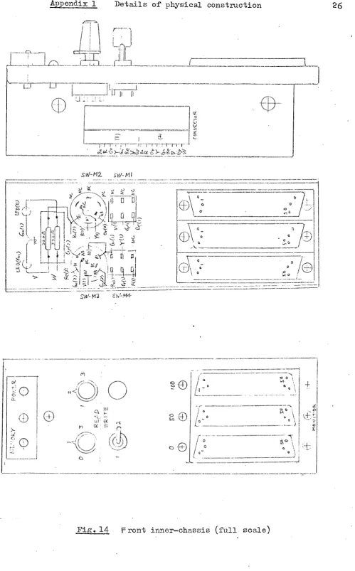
Fig. 13 shows the construction of the memoiy cabinet. Its details are shown in Appendix 2 (Figs. 14 to 21),
Fig. 29 (Appendix 4) shows a part of the front panel on which the controls and indicators are arranged. Fig. 14 shovm the front inner-chassis and Fig. 1$ shovis its circuit diagram.
The fi-ont inner-chassis consists of
S7/-M1 Writiiig mode selection
SY/-M2 Reading mode selection
SW-Wj) Reading period, selection
&),?-M4 Writing status
LED (Green) Poizer on
LED (Red) Data stored
Output monitoring terminals
The output monitoring terminals are utilized, irhen tlie memory is used for plotting numerical maps, for selecting the sampling time of the maps (see Ref. 3).
Fig. 16 shews the rear view of the PC-board frame on which 22 edge connectors and six 50-pin connectors for the output are arranged. These are divided into three identical groups, except for a board, MD-M1, which has different construction. These Triring connections are sheen in Appendi% 2.
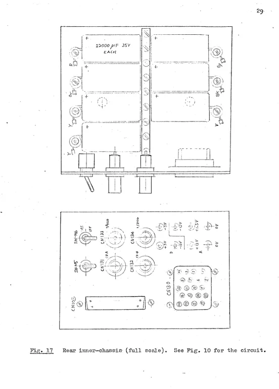
Fig. 17 shows the roar inner-chassis which contains connectors
CN103 From the tape reader CNI30 From the power supply
CNI31 From the internal clock, CR-A CNI32 From an external clock, GR-B CNI33 To a CRO (1/200 of the clock)
CNI34 To the numerical map plotter, "Qirough BD4 SW-MS Clock selection, A or B
SW-M6 Bias current for opto-electronic couplers Power supply voltage checking terminals
This chassis also contains internally seven 22000 )iP capacitors by which high-frequency oscillations assooiated with the long leads of the power supplies con be suppressed (their physical positions within the chassis are critical).
2
21
PE/R PANiL^ WITH fv4K/
-FEAR INNER CHAsaS
PC
fMWT WMEP
f%0W7 RAWcL
22
Printed, circuit boards
22 printed circuit boards which have three different constructions but all of uniform vridth (16 can) are used.
BD-M1 Main part of the control circuit BD-N5, BD«4ai2, ED-M19 Demultiplexers
(three boards are identical) BD-M2 to BD-M4
BD-M6 to BD-M11 SSEs, DACs, CCVs
BD-M13 to BD-KI8 (18 boards are identical) BD-M20 to BD-1122
Figs, I9a, 19b, 19o, 20a, 20b and 21 show the physical designs of these printed circuit boards.
Power supply unit
All the power supplies for the inputgmemory are contained in the oontiK)l table^ and cooled by a fan (12 cm , $0 litres per second).
!Phis unit and the memory cabinet are connected by a cable (2 m approz.).
7« Perfor-mszice
Table 2 shows a aummazy of performance of the input memory. Fig. 13 shows an example of overall linearity from the digital input of the input memory to the analogue output of a floating circuit, though its opto-electrcnic coupler.
The temporatui-e of the hottest components (integrated circuit packages of %ype 2511A on 3D-M2 etc., particularly those near the centre part of the cabinet) become higher than room temperature by about 22°C, with "Hie fan in operation.
8. Conclusions
A semicondictor-olrouit memoiy which satisfies particular requirements (a sin^e channel digital input, 140 channel parallel output each of which has different tine series of data in analogue and digital forma, igith current did.ving facilities for up to 700 opto-electronic couplers, and internal facilities for converting the order of data) for the electronic model for tides and stoim surges has been desired and constructed successfully.
23
Input
Storage
Output
Control
Accuracy
Linearity
Stability
Table 2 Summaiy of performance of the input memory
Form of data Mode 1: F(t) , or Mode 2: P(z:,y)j_.
-Dlgit&irpar^Lr'6-bit'^842r-6bde;'"^ 6 bits/word, one word/data.
Data Code
Control
Channel
Wilting speed
Digital, parallel 2-bit code. See Table 1.
Parallel 8-bit sin^e.
0 to 2 z 10 words/s, including random
internals, depending on an external data, e.g. Speed of data reader Writing time for 28E w.
(words/ s)
500 56 8
100,000 0.28 8
Terminals
Capacity
Max. period
TTL logic.
6-bit z 200 time-increments x 140 channels = 168K bits.
As long as power supply is continued.
Form of data j Continuous F(t),
Type Analogue current, signal (2 mA pk-pk maz.) + do bias (10 mA), for driving ]jEDs (infra-red).
Reading speed
Repetition ;
I
I I
Terminals
0 to 10 words (ecuivalent)/s
All channels can be read in parallel, in synchro-nization and i-epetition, 'ivith intervals of zero
(Mode O), T (Mode 1) or 2T (Mode 2); where T is a duration of 200 words equiYalent.
Current output (independent of external impedance) output impedance less than 10 for DC to 10 kHz. ,
Programmed ! Start, stop of writing and reading, and omission
i of wrong words etc.
Manut-l Selection of 2 writing modes, 3 reading modes, and the period of the reading dock.
^plitude
Frequency
Relative accuracy: max error jjO.T^ of full scale.
DC to 10 kHz (-:; db to 1 kHz)
Better tlian 1/o of full scale.
Temperature I T^loally 0.002/6 per for DAC (O to 40°G)
Power line I 1/b against +10^ input change
24
1.0
-p •H A •H O to .s "ts o t—I 0) 0 - P 1 g O Id 85• 6
i ! I •
* . . k . _ L .
±L r:;:T
. 4
4 i-i-r
ri-fe
, i . . . . .
' r
L. f_.
:5±I-i ±
L :r:
r
r
-:::r•:::T
i-t-'-j "I
id
.2
tn
:u - U
r %
i; r :
"T-. i • .
.:-i
J. .
L_L.H. 1- .
L-•• H.rr
• r
•—r-;-:
t; r
-m x t—- r
r u f
.
,
' : : : •Lfi. LLd::i.r
! • i \ • ! ! : !i n :
• ^ r
: :
. I , , I . . . .
! ; i • . ' ! - : : i- '
, : 1
. 1
f '
-r r
. , p
.ht" H
rr
/ r \
-M-f-r-
rr-xr
rr:
y ± I ::vi: :
H zcc; T-r t;.i. :•
iili -i-i. ! •'-+ _ J LI"rr ! -.•17:
: t_i_
r-.
-
, . ,
jJ-M
1 ,
r r
IH:!
m.k.. I f
-'' Lr^
1 ; ;
n-ir
t1
t :::.!: _ H E rr r-tr; I B IL _ L
r r - r r:r;!
i 1,1
:a
x:
.,i ! .^1
-t
•-- •-- f .
iipi; Itr :3iri
10
20 30 40Digital input
50 60
Fig* 13 Overall linearity from the digital input of the input. memory to the analogue output of a floating circuit, through lis opto-electronic coupler.
25
Aokncwle&frement
The author would, like to thank Mr J. Smithers for his considerable contributions in making the prototype of this memory, and adjusting and testing the actual memory.
References
(1) Ishiguro, S. (1972)
New electronic sea model,
Progress Report, from Jan. tc^ Dec. 1972, pp.
(2) iBhiguro, S. and Smithers, J. (1973) Mew electronic sea mod.el,
Progress Report, from Jan. to Dec. 1973, PP* 88.
(3) Ishlguro, S. (1976)
Numei-ical map plotter,
Appendix 1 Details of physical construction
26
r-— iTpl
CO c r
r~
%
'dini
-r i 1,:: irr-p^c«i.o )~\s o
1^'
4 j
kj
&
, :k
x .x:. ^ \! k
3:
0 n D 0
"Z .1 \5 >
, l t - u
2m/-m3
s>,'-.m4-o
1 0
©
ro
a r ura
o
# 0
s @
o @ a'
r
« 0 \ ln
& \
4-" 1
o
[image:28.595.62.562.25.829.2]\ : ±
interval ?d-mi
potvcr ow i led
-:a
-/\/v— 220^
m5mo%y : red lej)
I
a -/-x/va— 33an
m&morr ekath
x 5: r/v-am H-I
a..
Cl.,
y/vit)//& mucr
i :
s vv - m i
p.v.w,v4 Q '
I
^-eriod 21 g
ac
rV
,<1 1 4^r
_.^c_f j i bi wc
_L 2.
lal
r
bn (1) f
-0 1' ci '
:(+rv-> w
-0 — ^ u 22 ; b[>-w
(tc. bsc
i rfu
! y(u
i 6>-,' I}
' a\ ac
r! f o si
- vc
T
-n24-i $0:,'::! -n24-i ^
— l j
^—l—klcu—l r/!6 j -3—;—^djj J/2.7 i 6a_(aj a/ 2 j •
! ffj)
y- > wl?
nt7 <
«- e3
,
t"'-i t"'-i ckjt)
^ l i z j
4i , fiz
C f6 fe'z)
- c i 9
A 3 \
ac
k l _i_y_j^| cq- i
jy.
i i
27
28
cl-j 21
m l) \a n 09
cv22
i cw33 i o % n m ^ (a
cn;2+
ch/25 v) fs. 00 qt" o —
-— ^
3
cu26
oo\m / \ v o t k : 7
J'7 "t=f tdi
i x / / / / % / / % / / / / / / / / / / ^ x / % / / / y / / x / x / / / / y / / / / x > / / x / / / x / / / / x / 7 x _ ^ -x /l / x _ —i-—^ x X / X - X X X X X i ^ i; 2 - X / / X x
Fig. l6 (a) Rear view of the PC-hoEird frame with the output connectors (schematic, arbitrary scale)
(b) Detailes of the first section of the fziame containing
29
22000/'r jry
E A C H
b
'6' 2 u
- 4/^3 i."::
i - ,T\ \ 3.
a
#},
: >v \
-^.'t
u
"[co) \ ^ ' ~o
ig. @ g) ^
' % / '
r!a (m re?) :® 's) (£•
&
[image:31.596.25.578.28.799.2]vv
tfr
oj o
31
3 m ix)
n' <5
0.^
e
c = ]
3s q
o
oo o
cs n
^ ^4:
i
o
0. o/juoo q
o.y/ w
»<
n
u
c.o///#
j q
l i
e
?
ino m
(j-
-k o
a
$
m o.
©
9-
/0/cx/4-il II r i 1 r
II
_ll _ljnr o
in
0 . ^
m
o v ,
-h
1 , I
s cs h s, g te 1 1 » ^a:
co (/) lg
$ 0
1 1 » ^a: co (/) lg
' s i
„
ssfjiasi% y c^c -.(sri'<i-'-0^ s.bo&i
32
tS-A- C 3 J
§
oo cir &
m
ik-ootplit
%
%
<J : •• ^ I ^ I
"" i output
! - * <
/upur
B:%8gi o q lami
k
OUTPUT
§
r~9o <>^o ^(x rntfin v
e)6/7-p6/t
Fig, 20 Sub-control circuit board (3 boards identical),
33
?
xi ql_j e
//,4
r i n
#
7s-iia(li)
74?
7/^k
J
-(y+)
I
cz::
c : 3
c::^
c : = :
c z :
-c=:3
?
"k
D ^ ^20
0 2j?0
I •'f [
220
D l
~6 %
ick
2^a
u
© 1
l z ] /ca
izztj
c z d /<)fi'y4v
Or, ^
DATA
OUTPUT
u] in r( :iii
I
— <^ r<1 ^Lovi -j- tfjvo N I 111 L
pvata
_jjjput i g
I t t l l
do
PATA
OUTPUT k,
i -. 4
34
a-npendiz 2 Tables for internal connections
All the corrections are permanent. These tables are necessary only for the construction of the instrument or its servicing.
t a m e 3 Connection between CIT130 and circuit boards
Voltage OV +5v i -12? 4-15v -15v +27
i CN130 1 - 8 9-12 j 13-16 17 18 1 19 20
i P i n No., 1
' —:
1 P i n No ^ ' i
-— i'
i 5D-M1 c36-40 ol-5^^
BD-I42 3 5 1 5 1 4 1 7 26 25 24
BD-{.13 35 15 14 17 26 25 24
B M 4 35 1 5 14 17 26 25 24
o20 c21 - - -
-35 15 14 17 26 25 24
BD-517 35 1 5 14 17 26 25 24
BD-f.lS 35 15 1 4 17 26 25 24
35 15 14 17 26 25 24
BD-filO 35 1 5 14 17 26 25 24
BD-*.I11 35 1 5 14 17 26 25 24
BD-ia2 o20 c21
„
--3D-^a3 3 5 1 5 1 4 17 • 26 25 24
BlWul4 35 15 1 4 17 26 25 24
BD-zag 35 15 14 17 26 25 24
BD-ICL6 35 1 5 1 4 17 26 25 24
BD-M17 35 15 1 4 17 26 25 24
BD-M18 35 15 1 4 17 26 25 24
BD-)'119 c20 c21 - - — -
-BD-M20 35 1 5 14 l6 26 25 24
BD-]'.121 35 1 5 14 16 26 25 24
BD-1.122 35 1 5 14 16 26 25 24
For^ example, CNi30 Pin H o s . 9 to 1 2 have the voltage of 4-^, and/connected to BD-ZIl Component—side Pin Nos. 1 to
3 5
T a b l e /]. Connection bet-^reen BD-Kl and. other p a r t s
F u n c t i o n
8
7
6
I n p u t 5
3
2
^ / c r
1
2
3
4
5
. R I'lode 2 ^ K o d e 3
f e
RlH) SOL
outtyut
KEG
(cw2)
R 2 C
R e s e t S t aj?t
b C d A A ^ 2 a / 6 x 7 ^ 8 bd-wl p i n _ n o .
1 2
3
4
5 67
j 8
; ^
; 10
! 11! 1 2
I 1 3
i 1 4
i 15.;. .
1 1 6
: 17
. : _ _ 1 8 . .
19
: 20
21 .
2 2 ;
23
24
_ 2 5 2 6 _ 27 2 8 29 30 .31. 32 33 34 35 36 37 38 39 _ 4 0
clr-o cl6 cl7 ol3 cl9 g2q;
Part connected.
c m o 3 / 8
7
65
4
3
2 1 sw-ml/1'Pin 18 ^
Pin 19 Pin
P i n P i n P i n
20
21
22
23
i n e a c h o f
B D - M 2 to B D - M 4
3D-M6 to B D - K l l BD-M13 to B D - K 1 8 BD-H20 to B D - M 2 2
'sw-)'il/2" ' SW-i=I2/A2 sw-h2/&1
CIT103/9
C E 1 0 3 / 1 0 , C I T 1 0 3 / 1 2 sw-io/b
Pin 15 in each of
Pin 2 2 in each of
P i n 17 in each of
i n each of BIW.!5, BD-1H12, B M I 9
b i w a 9 / 7 4 1 5 4 ( 9 ) p i n
SW-M4
SW-Ml/C __ _
P i n 17 i Pin 1 8 P i n 19
P i n 1 6 .
bd-ii5/23
b ] h a 5 / ^ 4
bd-4.15/25 bd-;h2/23 bd^^il2/24 BD-3!12/25 BD-MI8/23 biw.ii8/24 bd-i.i18/25 +5v SW"M3/A3 sw-3j3/b1 sw4.13/b2
s w ^ . o / b 3
w V B e G n y O r R B n
B e ( l )
BD-i;5, BD-1.112, BD-ia9
BD-K5, 3 D - M 1 2 , BD-I.1I9 .BD-M2 to B B - H 4
BD-Ho to 3 D - H 1 1 BIM'i13 to BD-J418 BIM.120 to BD-^.i22
1 4 ...
V ( l ) O r ( 2 )
R ( 2 )
B n ( 2 ) or/e:r
G y / B e
g y . . . T( l )
g x l )
W/R
}7/0r
w / g y
W / G n . B n O r t G n B e v g y
w i
i i
gnl2)'
B e ( 2 ) V ( 2 )
g y l 2 )
w / b n
36
'fable 5' Connection bettveen B D - K 1 2 or BD-*'ll9
and. other ci
r
|:BD-M51 Colour
i - .
i
p i n H o .1 Colour
i - .
i
p i n H o .1
B n !' 1 M 2 / 1 0;
i 2 11i
O r:
3
1 2_ Y 4 _ _.13
: B n
ii
5 M 3 / 1 0: R
!i 6 11O r
;
7
1 2%
b
1 3: B n
9
M 4 / i o^ R 1 0 1 1
Or' :
1
]1
1 2: Y
: 1 2 1 3B n
i
^9 M ^ 2 7! ^ ! 30
28
! O r ! 31'- 29
: 1
i 32 30B n ' 3 3 " K 3 / 2 7
! E : 34 28
O r !. 35 29
Y
36 30'Bn
; 37
314727R
il
38 28: O r :: 39 29
1 .: 4 0 _ 3 0
M 6 / I O
" B n 1
3 0 M 6 / I O
R 2 11
Or
3
1 2t 13
B n M f / l O
: E 6 11
O r ' 7 1 2
Y 8 13
B n
:
9
K 8 / 1 OR ! 1 0 11
Or 1 1 1 2
' Y 13
29 i K 6/ 2 7
R !: 30
i
28- O r 31 i 29
Y 32...
_1.
. _ 3 0: B n " 33 i M 7 / 2 7
a
; 34
i
2 8O r
35
i
29. T 36...._ L
_3a
""Bn : 37
I
M 8 / 2 7; R 38 1 28
O r 1; 39 ; 29
1 T 30'
^iw.112
p i n No,
bd-i419
p i n I f o .
K l O / l O
M l 8 / i O
m l l / i o
30 m i 8 / 2 7
28
K i 3 / l 6
t i ^ / i o m i 4 # d
% / i o
)0
K 1 4 / 2 7 28 29
30 m l 5 / 2 7
28
29
30
F o r example, P i n No,
b y the B r o ™ Trlre.
37
Table g' Connection between the output terminals and each of
BD-I:I2 to 3D-H4, BD-M6 to BD-Kll, BD";.113 to BD-^-IlS, and BD-M20 to BD-M22.
j ! CIT21 CN22 CIT23 ' Clf24 C E 2 5 GN26 , P i n No_
M9/31 M l 6/1
Bn : 1 M 2 / I M2/31 H9/I M9/31 M l 6/1 Ml6/31
R : 2 2 32 2 32 2 32
Or : 3 3 33 3 33 3 33
T 4 4 34 4 34 4 34
Gn 5 6 36 6 36 6 36
Be 6 7 37 7 37 7 37/
? 7 8 38 8 38 8 38
Gy 8 9 39 9 39 9
^ " B n " " ]lQ M6/1 M6/31 MI3/I 1 Ml3/31 M 2 0 / l M20/31
R 11 2 32 2 32 2 32
Or 1 2 3 33 3 33 3 33
T 13 4 34 4 34 4 3 4
G n 1 4 6 36 6 36 6 36
Be 1 5 7 37 7 37^ 7 37
V 16 8 38 8 38 8 38
Gy 17 9 39 9 .. ,39.. : ,9 ,39
Bn 1 8 M3/1 K3/31 KlO/l 1:10/31 K 1 7 / 1 M17/31
E 19 2 32 2 32 2 32
Or 20 3 33 3 33 3 33
Y 21 4 34 4 34 4 34
Gn 22 6 36 6 36 6 36
Be 23 7 37 7 37 7 37
7 24 8 38 8 38 8 38
Gy 25 9 39 9 39 9
Bn M7/1 K7/31 KI4/1 MI4/31 K 2 1 / 1 M21/31
R 27 2 32 2 32 2 32
D r 28 3 33 3 33 3 33
Y 29 4 34 4 34 4 34
Gn 30 6 36 6 36 6 36
Be 31 7 37 7 : . 37 7 37
Y 32 8 38 8 38 8 38
Gy 33 9 39 9 39 . . ,9 39 .
" B n ^ ' 34 k 4 / l K4/31 Kli/i Kll/31 K I 8 / 1 , KI8/31
R 35 2 32 2 32 2 32
Or 36 3 33 3 33 3 33
T 37 4 34 4 34 4 34
Gn 38 6 36 6 36 6 36
Be 39 7 37 7 37 7 37
V 4 0 8 38 8 38 8 38
Gy 4 1 9
M 8 / 1
-39 9 39 ' 9,., : _ 39
' "Bn ^ 3
-9
- M 8 / 1 - m8/3l M l 5/1 ^15/31 ! M 2 2 / 1 ' K 20/31
E 4 4 2 32 2 ! 32 2 ! 32
Or 45 3 : 33 3 i 33 3 33
T 46 4 34 : 4 ^ 34 4 34
Gn 47 6 36 : 6 36 6 36
Be : 48 7 37 ; 7 37 7 37
V 49 8 ; 38 ! 8 38 8 38
Gy 50 9 39 : 9 39 9 39
For exanple, 03^21 Pin ITo. 1 is connected, to BD-).i2 Pin It) , 1,
Table Conection between Tape reader 26C and the input
memory through C1T103 , , . _
I BD30 Cable CIT103 ' Memory
; P i n N o . I (Gy)
Function
Data, ohannel 1
2
3
4
5
Control ohannel
7
_ 8
^Tape feed hole) FlfD (Tape forward) BWD (Tape backward) SOL (Clutch solenoid) Common (OV)
+5t Screen
3
5
7
9
11 j o 19 21 29 23 25 27 15-16 171 0 - 1 2 ; 2 1 - 2 5
Bn r Or I Gn Be V Gy w R/Gn R/Be T/Be
P i n ITo. internal
1
23
4
7
8
9
1011
12 Gn(D).kPk 13B k 25
Bn R Or Y Gn Be V gy w Y/R R/Be Y/R * lf(T) t
* Connected
Table 8 Conection between Tape reader 26C and the contol
cabinet
Function Tape-reader
internal connector Pir No.
Motor drive, +24V Common, 0\r
Screen '
13 14-17
10-12, 21-25
Cable(W)
Rc m 6
Pin Fo.
L
it
Connection between BD30 end the internal connector of Tape reader 26C
Function
Data track
Control track
fe FWD BWD bol
Common (07)
1
23
4
5
6
7 8Tape reader
internal connector P i n No.
1
23
4
5
6
7 19 2010-12, 21-25
[image:40.595.56.538.51.789.2]39
Table IlQ. Memory channel ITo», Output, channel ITo ., and Monitoring terminal Ho.
3^ The memory is -vrritten automatically in the order of Memory channel Ho,
2 The Memory channel Ho. is indicated at the end of each peir of wires inside the main network cabinet,
2 Each Monitoring terminal is connected to the first pin of each Output channel, and the same wire colour is used,
^ Pin Hos. 9 and 42 of each Output terminal are not used.
^70
•f-/
1 - ^
•_£> JO ico^ MOWiTnPi M & -f E K'Mif-MuS
(tiioi-.'t
70 t v
i k " 4/
rt •i 1 a i' 1 d! u L cai
»—
/.
cns 2.
(. memotv fae'wzt )
y
vzl
Pig. 22 Key diagram for tables
Memory
i channeli Ho. 1 Pin Ho. Wire colour
o : 1 - 2 Bn-S
i 1 ! 3 - 4 Or-Y
! 2 i 5-6 Gn—B @
1 3 ! 7 - 8 V -Gy
i 4 ; 18-19 Bn-S
1 5 i 20-21 Or-Y
I 6 ; 22-23 On—Bo
i T ; 24-25 V -Gy
1 ~ a 1 34-35 Bn-R
9' ! 36-37 ! Or-Y
i 10 38-39 ! On—Be
11 40-41 i V -Gy
1 2 10-11 ; Bk-Bn
13 12-13. i R - Or
1 4 14-15 : Y -Gn
1 5 16-17 Bn-R
16 26-27 W - B k
17 2 8 - 2 % Bn—H :
18 30-31 Or-Y :
19 32-33 Gn-Or i
20 43-44 Bk-Bn
21 45-46 R -Or
22 47-48 Y - O n
23 49-5Q' Y - G n
Output terminal | Circuit Connector I board Ho.
Monitoring | terminal Ho.i
B D - M 3
CN21
bd-m4
ed-m6
bd-m7
s d ^ 8
(100) 40
(0> 1 2 3 4 5 6 7 6
9
1011
12 13 1 4- i i
17
18
_ 1 9 _
20
21
22
40
Memory OutDut teriainal
channel ITo. Pin ITo. Wire colour! Connector
2 4 1 0 - 1 1 Bk-Bn j
25: 12-13 R - Or 1
26 14-15 T - G n
27 16-17 Bn-R I
28 26-27
29: 28-29 Bn-R 1
30 30-31 Or-Y 1 :
31 32-33 Gn-Or ' !
32 43-44 Bk-Bn ;
33 45-46 R - O r : :
34 47-48 T - G n i '
3 5 4 9 - 5 0 1 CF22 i
1 - 2 Bn-R ; :
37 3-4 Or-T : ,
38 5—6 Gn-Be' ' I
39 _ . 7 - 8 V - G y i !
4 0 18-19 Bn-R ' i
41. 20-21 Or-T i !
4 2 22-23 Gn-Be i
43 24-25 . . V - G y ; l
4 4 34-35 Bn-R
4 5 36-37 Or-Y ;
46 38-39 G n - B e :
47 40-41 V - G y i I
4 8 1 - 2 Bn—R ! 1
49 3-4 Or-T !
50 5—6 G n — B e : 1
51 7 - 8 \ _ - G y . j l.
52 18-19 Bn-R
53 20-21 Or-Y ' :
54 22-23 Gn—Be ' 1
55 24-25 V _^y ; i
56 34-35 Bn-R : :
57 36-37 Or-Y : i
58 38-39 Gn-Be 1
. 59 40-41
6 0 10-11 Bk-Bn Ca23 i
621 12-13 R - Or : !
6 2 14""15 Y - G n : j
63. 16—17 Bn-R i i
64 26-27 ' W - B k " ' !
65 28-29 Bn-R ! !
66 30-31 Or-Y i .
67 32-33 Gn-Or i i
68 4^-41 Bk—Bn ;
69 45-46 R - O r ! :
70 47-48 Y - O n : i
jl _49-r50_ Y - G n ! i
Circuit b o ard. No,
Monitoring terminal ITo,
(0)
: ]3d-;.ia
41
Hemoiy chBiinel ITo,
Output terminsl ; circuit
P i n ITo. Wire colour Connector "boarcl Eo,
Monitoring I t e m i m a l ^0.:
7 2 10-11 Bk-Bn : (50) 22
73 12-13 R - O r
BD-I-l 13 1 23
7 4 14-15 Y - G n BD-I-l 13 24
.75 16-17 Bn-E ' 25
76 26-27 W - B k 26
77 28-29 Bn-R : 27
78 30-31 O r ^ BD-I114 28
79 32-33 Gn-Or 29
8 0 4 3 — 4 4 Bk-Bn : 30
45-46 R - O r • ; 31
8 2 47-48 T - G n ! B])-i4l5 32
83 8 4
__49-50._ _ 1 - 2
T - G n
Bn-R Gn24 ;
33 34 8 5 8 6 3—4 5—6 Or-Y
Gn-Be BD-tI9
35 36
_ 87 _ .. 7 - 8 . .7 . - G y 37
88 18-19 Bn-R 38
89 20-21 Or-Y
: BD-IIIO 39
9 0 22-23 Gn-Be : BD-IIIO 40
9 1 . 24-25 V - G y 41
9 2 34-35 Bn-R 42
93 9 4
36-37 38-39
Or-Y
Gn-Be BD-i'111
43 < 4
9 5 40-41 V —Gy : 45
96 1 - 2 B n - R 46
9 7 9 8
3-4 5-6
Or-Y
Gn—Be : BD-KI6
47 48
9 1 _ 7 - 8 V - G y 49
1 0 0 " 1 8 - 1 9 '"'Bn-R 50
101. 1 0 2
20-21 22-23
Or-Y G n — B e
•
B i w c i y ' (100) 1
2
— 1 0 3 _ 24-25 T - G r
— — - ^
3
1 0 4 34-35 Bn-R i 4
105 36-37 Or-Y
I BD-a|8
5
106 38—39 G n — B e I BD-a|8 6
lOTf 40-41 V — G y _ 7
1 0 8 10-11 "iBk-Bn C1T25
109 12-13 R - O r
; BD-I'130
9
1 1 0 14-15 Y - G n ; BD-I'130 10
lllL 16-17 Bn-R : 11
1 1 2 26-27 W - B k : 12
113 28-29 Bn-R
: BD-)'121 13
1 1 4 30-31 Or-Y 14
. 115^^ .3.2-33 Gn-Or _ _ 15
1 1 6 43-44 Bk-Bn 16
117 45—46 R - O r 17'
118 47-48 Y - G n 18
42
Memory Output terminal Circuit
chann.el No. P i n . Nc . Wire colour 1 Connector board No
1 2 0 10-11
121 12-13 R - O r !
B[D-^Jl20
122 14-15 T - G n 1
123 16-17 Bn-R
1 2 4 26-27 W - B k
1 2 5 28-29 Bn-R
BD-0j21
126 30-31 O r - T BD-0j21
127 32-33 Gn-Or i
1 2 8 43-44 Bk-Bn 1
129 45—46 a - O r 1
B D - M 2 2
1 3 0 47-48 i T - G n B D - M 2 2
1 3 1 49-50 T - G n I
GIT26 i
1 3 2 1 - 2 B n - R i GIT26 i
133 3 - 4 ; Or-T 1
B M 1 6
1 3 4 5—6 Gn—Be B M 1 6
1 3 5 7 - 8 V -Gy :
136 18-19 Bn-R
137 20-21 Or-T i
BD-I417
138 22-23 Gn-ae ! BD-I417
139 24-25 V - G y 1
34-41 Not used i
terminal ITo.
(100)
2021
22
23
24 25 26 27
28
29
30 31 32 33 34 35 36 37
3w
39
Function Monitoring
terminal Eo,
TaDG reader out-out , channel 1
2
3
4
5
6
7
8
Writing clock Reading clock
(W)
(Bk)
(100)
41 4 2 43 4 4 4546
47 48 49
50
Note Signals can be observed at the monitoring terminals, only