Available Online atwww.ijcsmc.com
International Journal of Computer Science and Mobile Computing
A Monthly Journal of Computer Science and Information Technology
ISSN 2320–088X
IMPACT FACTOR: 6.017IJCSMC, Vol. 7, Issue. 6, June 2018, pg.31 – 36
Design of Low Power and
High Speed Full Adder Cell
Using New 3TXNOR Gate
Pramod Aladale
Department of Studies in VLSI Design & Embedded System Engineering, VTU Belagavi, India
Abstract- In the current age of technology advancement it is necessary to design different new concepts to
reduce area of the cell as well as power consumption. The adders are always meant to be the most
fundamental requirements for process of high performance and other multi core devices. In present work a
new XNOR gate using three transistors has been designed, which shows power dissipation of 0.03866W in
90nm technology with supply voltage of 1.2V. A single bit full adder using eight transistors has been designed
using proposed XNOR cell and a multiplexer, which shows power dissipation of 0.07736W. It is implemented
by using synopsys tool(version-L-2016.06-8) using custom compiler with 90nm technology.
Keywords- CMOS, exclusiveNOR (XNOR), full adder, low power, Logic gates
I. INTRODUCTION
substantial improvement in power consumption, speed and size, but at the cost of weak driving capability and reduced voltage swing. However, reduced voltage swing has the advantage of lower power consumption [2].
Initially the electronics started their evolution with the invention of vacuum tubes. But with the help of Vacuum tubes only the movement of electrons were studied. After vacuum tubes transistors and diodes were introduced. But for larger circuits it was difficult to fabricate them in a board as they occupied larger space and consumed more power. The full adder circuit performance is dependent on the approach for designing the circuit. The speed of operation of a circuit is indirectly found with the help of delay time calculation which directly depends on the transistor count, the logic depth and other criteria. The power consumption depends on the switching activity and the number and the transistor size. The transistor size and routing complexity helps to know the area of a die. Circuit realization for low area has become an important issue with the growth of integrated circuit towards very high integration density and high operating frequencies. Due to the important role played by XNOR gate in various circuits especially in arithmetic circuits, optimized design XNOR circuit to achieve small size and delay is needed. The primary concern to design XNOR gate is to obtain low power consumption and delay in the critical path and full output voltage swing with low number of transistors to implement it. A survey of literature reveals a wide spectrum of different types of XNOR gates that have been realized over the years. The early designs of XNOR gates were based on either 4 transistors [3] or 3 transistors that are conventionally used in most designs. Full adder acts as the basic block of all adders which are used to perform multi bit additions. There are also various ways to design the Full Adder circuit in terms of CMOS logic. With increasing demand in speed and power, our main aim is to design Full adder circuit so that it consumes less power and faster. Most of the power in any circuit is being consumed by the power given to the data path of the circuit which consists of the transistors. Hence by reducing the number of transistors we can reduce the power consumption also by reducing the data path, the circuit can be made faster.
II. METHODOLOGY Conventiona10T Full Adder:
The schematic of the conventional 10T CMOS full adder is shown in Fig 1.The 10T CMOS full adder circuit design is optimized to consume less power and less fabrication area with lesser internal capacitance. Respective simulation results showing the output waveform and output power of 10T full adder design with 90nm CMOS technology are depicted in fig.2 and fig.6.
PROPOSED FULL ADDER:
Basic Building Blocks
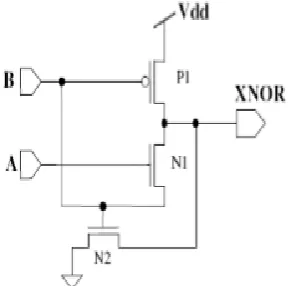
1. Three Transistor Xnor Gate:
The XNOR gate (sometimes, EXNOR, ENOR, and, rarely, NXOR, XAND) is a digital logic gate whose function is the logical complement of the exclusive OR (XOR) gate. A high output (1) results if both of the inputs to the gate are the same. If one but not both inputs are high (1), a low output (0) results.
Fig 2: Existing 3T XNOR Gate Table1: Truth table of XNOR logic gate
Fig 3: Proposed 3T XNOR Gate
Xnor Gate Working:
In the proposed XNOR cell 1 PMOS transistor and 2 NMOS transistors are used as shown in figure3. The system‟s behavior for different inputs are described:
Whereas the NM0 and NM1 passes a strong „0‟ and a weak „1‟. The functionality of the 3T XNOR gate is described below:
Case 1: When A=0 and B=0. When both the inputs are at 0V, the NM0 and NM1 are turned OFF the VDD appears across the PMOS. This results in an 1V output across the output terminal Y and GND
Case 2 and 3: When (A=0 and B=1) or (A=1 and B=0). When either of the input is „1‟ and the other is „0‟. The
NMOS which is turned ON will pass a strong „0‟ to the output. This results as „0‟ for both the cases.
Case 4: When A=1 and B=1. When both the NMOS are turned ON by providing „1‟ for both the input
terminals, the output across the output terminal is generated by both the NMOS and PMOS. The NMOS generates a weak „1‟ whereas the PMOS generates a strong „1‟. As a result, a strong „0‟ is obtained at the output. The output waveforms of proposed xnor gate is shown in Fig 5.
III.
DESIGN & IMPLEMENTATION OF FULL ADDER CIRCUIT
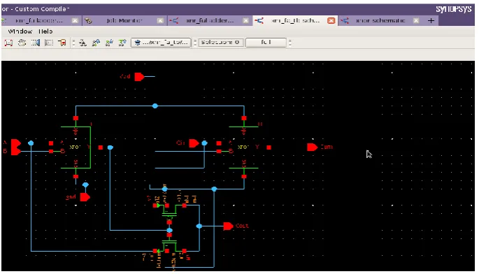
Full adder circuit can be implemented with different combinations of XOR/XNOR modules and two multiplexer but this approach has not been used in current work as XNOR/XOR cell shows high power consumption than single XNOR gate. Proposed full adder circuit has been implemented by two XNOR gates and one multiplexer block as shown in Figure 4. Sum is generated by two XNOR gates and Cout is generated by two transistors multiplexer block. The single bit full adder using proposed XNOR gates with eight transistors has been implemented and shown in Figure 4. For multiplexer section typical values of width (Wn & WP) 0.23µm & 0.23µm for NMOS and PMOS transistors have been taken with gate length of 0.9µm. Simulations have been performed using SPICE based on SAE( Simulation and Analysis Environment) 0.9µm CMOS technology with supply voltage of 1.2V.
IV. EXPERIMENTAL RESULT
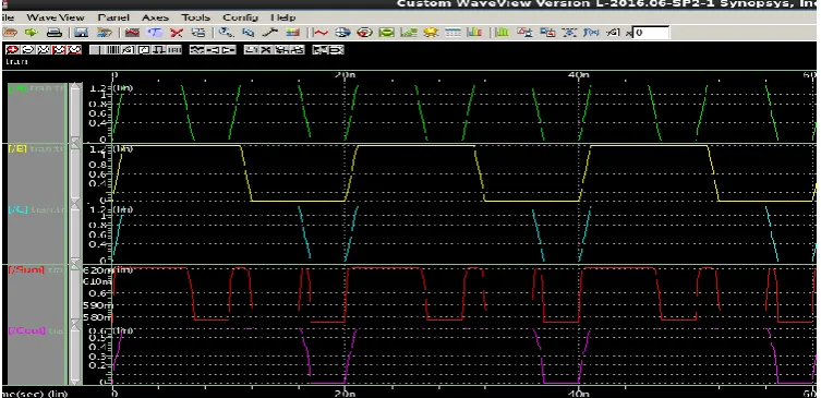
Output wave forms of conventional and proposed Full Adders are shown in Fig 6 and Fig 7.
Fig 5: Output Waveform of proposed 3T XNOR Gate
Tabulation of Simulation results:
Table 1: Xnor Gate
Supply Voltage (V) Power Dissipation(W)
3.0 0.62536
2.5 0.377959
2.0 0.210017
1.2 0.03866
Table 2: Proposed Full Adder
Supply Voltage (V) Power Dissipation(W)
1.5 0.178589
2.5 0.756103
2.0 0.4200
1.2 0.07736
V. CONCLUSION
In this proposed paper, a new low power XNOR gate using three transistors has been presented, which shows power dissipation of 0.03866W in 90nm technology. Compared with earlier reported XNOR gates, proposed circuit shows less power consumption and better output signals with reduce transistor count. A single bit full adder using eight transistors has been designed using proposed XNOR cell, which shows power dissipation of 0.07736W. Power consumption of proposed XNOR gate and full adder circuit‟s shows better performance in terms of power consumption and transistor count.
REFERENCES
[1].D. Radhakrishnan, “Low-voltage low-power CMOS full adder,” in Proc. IEE Circuits Devices .Syst., vol. 148, Feb. 2001, pp. 19-24. [3] Y. Leblebici, S.M. Kang, CMOS Digital Digital .Integrated Circuits, Singapore: Mc Graw Hill, 2nd edition, 1999, Ch. 7.
[2].J. H. Kang and J. B. Kim, “Design of a Low Power CVSL Full Adder Using Low-Swing .Technique”,.ICSE2004 Proc. 2004, Kuala Lumpur, Malaysia.
[3].H. T. Bui, A. K. Al-Sheraidah, and Y.Wang, “New 4-transistor XOR and XNOR designs,” in Proc.2nd IEEE Asia Pacific Conf. ASICs, 2000, pp. 25–28.
[4].H.T. Bui, Y. Wang, Y. Jiang , “Design and analysis of 10-transistor full adders using novel XOR-XNOR ….gates,” in Proc. 5th Int. Conf. Signal Process., vol. 1, Aug. 21–25, 2000, pp. 619–622. [5].H. T. ….Bui, .Y. Wang, and Y. Jiang, “Design and analysis of low-power 10-transistor full
adders.using XOR-….XNOR gates,” IEEE Trans. Circuits Syst. II, Analog Digit. Signal Process., vol. 49, no. 1, Jan. 2002, ….pp. 25– 30.