DALAL, ISHITA U. An Efficient FPGA Implementation of the Discrete Wavelet Transform. (Under the direction of Professor Winser E. Alexander).
Rapid growth in the multimedia and communications industries is fueled by the development of hardware architectures for high performance signal processing
algo-rithms. Implementation of computationally intensive DSP algorithms has become a popular application area for digital hardware platforms such as ASICs and FPGAs.
This research is directed towards improving the hardware performance of discrete
wavelet transform (DWT) as a case study of DSP application that requires intensive
mathematical computations. The DWT is the transformation block used in the latest multimedia compression standards such as the JPEG2000 for still image compression
and H.264 for video compression.
This work presents the basis for designing an efficient implementation for a
multi-level 1-D DWT hardware architecture for use in FPGAs. The proposed architecture
systematically combines hardware optimization techniques to develop a flexible DWT architecture that has high performance and is suitable for portable, high speed,
power-efficient devices. The hardware optimizations considered include data-interleaving for
reduced FPGA resource utilization, polyphase structures for lower power dissipation and pipelining for high throughput applications. Several hardware designs with
dif-ferent combinations of optimizations and filter structures are designed, simulated and
synthesized on the Xilinx Virtex-5 FPGA. The impact of these hardware optimiza-tion techniques on the overall DWT hardware system are analyzed and the tradeoffs
between the pertinent hardware performance metrics: namely power, operating
fre-quency, latency and resource utilization, are investigated. We illustrate that a DWT
design using a pipelined and polyphase transpose direct form FIR filter coupled with data-interleaving gives the best combination of the performance metrics when
by Ishita Dalal
A thesis submitted to the Graduate Faculty of North Carolina State University
in partial fullfillment of the requirements for the Degree of
Master of Science
Electrical and Computer Engineering
Raleigh
2008
APPROVED BY:
Dr. William W. Edmonson Dr. W. Rhett Davis
DEDICATION
To
My late grandfather,
Naginlal M. Shah
my grandmother,
Sarojbala N. Shah
my parents,
Uday and Trusha Dalal
BIOGRAPHY
Ishita Dalal was born to Uday and Trusha Dalal on 24th June, 1984 in Mumbai, India. She received her Bachelor of Engineering (B.E) degree in Electronics from
D.J. Sanghvi College of Engineering (Mumbai University) in June 2006. She joined NC State University, Raleigh in Fall 2006 to pursue graduate studies in Electrical
Engineering. She has been working under the guidance of Dr. Winser Alexander as
a part of the High Performance Digital Signal Processing (HiPerDSP) Laboratory at
ACKNOWLEDGMENTS
My utmost gratitude goes to my advisor Dr. Winser Alexander for his expertise, unwavering support and patience throughout my research. His belief and confidence
in me was the affirmation I needed to take up and succeed in this challenge. He has helped me hone my ability to conduct research, write technical documents and
express my ideas. I have nothing but admiration and respect for him and working
under him was truly a rewarding experience.
This journey would have been nearly impossible had it not been for my friend and
mentor, Ramsey Hourani who was the torchbearer during the entire course of this
research. He was always there to meet and discuss my queries, markup my chapters and give me strength when I doubted myself. A mere thank you may not suffice all
the help he has given me.
I am grateful to my other committee members, Dr. Davis and Dr. Edmonson for
their valuable inputs. It was a privilege to be a part of the HiPer DSP lab and I am
thankful to all its members for sharing their research ideas and for the weekly presen-tations, especially Cranos Williams and YoungSoo Kim for helping me with LATEX. I would also like to thank Manav Shah for his constructive feedback, my roommates:
Jyoti, Ushma and Aruna for making Raleigh a home for two years, my close friends: Sapna, Ami, Shonan, Dhvani and Akriti for their encouragement and Rishik Jariwala
for proof-reading my thesis and providing me moral support during stressful times.
I am deeply indebted to my parents Trusha and Uday Dalal for their boundless love and for teaching me the true worth of education. I thank my sister Sonam for
her everlasting faith in me. A very special thank you to my late grandfather Naginlal
Shah and my grandmother Saroj Shah for their prayers and blessings, uncles Daxesh and Parag Shah for their priceless advice, aunts Raksha Thanawala, Bina and Roopa
Shah and my cousins: Mitali, Vighnesh, Parth and Arnav for their love and warmth.
TABLE OF CONTENTS
LIST OF TABLES. . . vii
LIST OF FIGURES. . . viii
1 Introduction. . . 1
1.1 Background . . . 1
1.2 Motivation . . . 2
1.3 Contribution. . . 4
1.4 Thesis Organization. . . 5
2 Background. . . 6
2.1 Wavelet Theory . . . 6
2.1.1 Wavelet Family . . . 8
2.1.2 Discrete Wavelet Transform . . . 9
2.1.3 Multiresolution analysis . . . 11
2.2 Implementation of DWT . . . 12
2.2.1 Convolution Based DWT . . . 12
2.2.2 Survey of DWT Architectures . . . 17
2.2.3 Lifting based DWT . . . 21
2.3 Chapter Summary . . . 23
3 Design Implementation. . . 25
3.1 Floating Point Implementation . . . 27
3.2 Fixed Point Implementation . . . 29
3.3 Hardware Implementation . . . 31
3.3.1 Hardware metrics . . . 32
3.3.2 Filter structures . . . 35
3.3.3 Introduction to Hardware Optimization Techniques . . . 38
3.4 Hardware Design Implementation . . . 45
3.4.1 Basic Implementation. . . 45
3.4.2 Polyphase Implementation . . . 47
3.4.3 Polyphase With Pipelined Implementation . . . 49
3.4.4 Hardware Implementation With Combined Optimizations . . . 54
4 Results and Analysis . . . 62
4.1 Bit Precision . . . 63
4.2 Virtex-5 FPGA . . . 64
4.2.1 ISE Project Navigator design flow . . . 65
4.2.2 XPower Estimator . . . 67
4.3 Results and Analysis . . . 68
4.3.1 Hardware Design Architectures . . . 68
4.4 Hardware Synthesis Results . . . 70
4.4.1 Area . . . 70
4.4.2 Throughput . . . 73
4.4.3 Latency . . . 74
4.4.4 Power . . . 75
4.5 Architectural Analysis . . . 80
4.5.1 Comparison of Architectures . . . 80
4.5.2 Analytical Comparison of DWT Architectures . . . 81
4.6 Chapter Summary . . . 82
5 Conclusion and Future Work. . . 84
5.1 Conclusion . . . 84
5.2 Future Work . . . 86
LIST OF TABLES
Table 2.1 Time Frequency Localization. . . 16
Table 3.1 Comparison of different Filter Architectures . . . 37
Table 3.2 Comparison of computations for polyphase and non-polyphase filters. 40 Table 4.1 Quantization Results for Fixed-Point DWT implementation. . . 64
Table 4.2 Design Architectures . . . 69
Table 4.3 Area Results and Percent Utilization . . . 71
Table 4.4 Throughput Results. . . 74
Table 4.5 Latency Results. . . 75
Table 4.6 Power Results for DWT architectures in design space. . . 78
LIST OF FIGURES
Figure 1.1 Basic Image Compression System. . . 3
Figure 2.1 Time scaling the wavelet function . . . 8
Figure 2.2 Time shifting the wavelet function . . . 9
Figure 2.3 Single DWT Block . . . 13
Figure 2.4 3-level 8 channel DWT decomposition . . . 14
Figure 2.5 Time-frequency graph for a 3-level 8 channel DWT decomposition . 15 Figure 2.6 Coefficient-Interleaving implemented by Marino et al. [1] . . . 18
Figure 2.7 Systolic implementation of a 3-Level DWT by Denk et al. [2] . . . 20
Figure 2.8 Parallel implementation of the 1-D DWT by Zhang et al. [3] . . . 21
Figure 2.9 The Lifting Scheme . . . 22
Figure 3.1 Design Flow . . . 26
Figure 3.2 Single Precision IEEE floating point format . . . 28
Figure 3.3 General FPGA architecture [4] . . . 33
Figure 3.4 Critical Path Delay . . . 34
Figure 3.5 Latency . . . 34
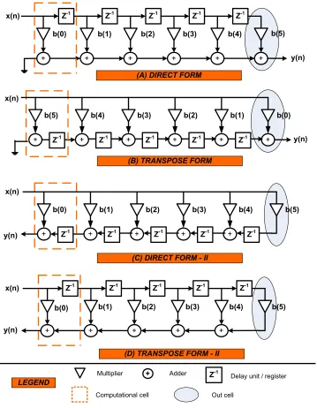
Figure 3.6 Block Diagrams for FIR Structures . . . 36
Figure 3.7 Filtering and downsampling . . . 39
Figure 3.8 Example of decimation by 2 . . . 39
Figure 3.10 Filter zero-interleaved by factor ’k’ . . . 42
Figure 3.11 Data-interleaving. . . 44
Figure 3.12 IO waveforms for a DWT algorithm . . . 46
Figure 3.13 Decimation by two . . . 46
Figure 3.14 Polyphase implementation for a level 1 low pass filter . . . 47
Figure 3.15 Polyphase implementation for a level 1 low pass filter . . . 48
Figure 3.16 Pipelined computational cell of a Direct Form (DF) Filter . . . 50
Figure 3.17 Pipelined computational cell of a Transpose Form-II (TF-II) Filter. . 52
Figure 3.18 Pipelined structures for level 1 polyphase structure (He). . . 53
Figure 3.19 3-level 8 Channel DWT structure with data-interleaving. . . 55
Figure 3.20 Our Method of implementation . . . 56
Figure 3.21 Pipelined computational cell of a Transpose Form-II (TF-II) Filter. . 57
Figure 3.22 Details of control structure C2. . . 58
Figure 3.23 Waveforms of control structure C2 . . . 59
Figure 3.24 Details of control demultiplexer. . . 59
Figure 3.25 Deinterleaving waveforms . . . 60
Figure 4.1 ISE Design Flow [5] . . . 66
Figure 4.2 Normalized Area Graph . . . 72
Figure 4.3 Toggle rates . . . 76
Figure 4.4 Power Graphs . . . 79
Figure 5.1 2-D decomposition of an image using the DWT [6] . . . 87
Chapter 1
Introduction
1.1
Background
Video and image processing algorithms have developed at a blistering pace in
the past decade and are giving rise to new innovations and applications. The new
genre of multimedia applications equipped with good quality video and images makes its presence ubiquitous throughout the internet and the mobile industry. A myriad
of multimedia applications, such as digital broadcasting, mobile video conferencing,
video streaming, HDTV technology, is a consequence of highly sophisticated and com-plex signal processing algorithms used in the core of this advanced technology.
Traditional Digital Signal Processors (DSPs) have limited capabilities for process-ing such high volume data efficiently at real-time or near real-time rates. The trend
is shifting towards the use of Application Specific Integrated Circuits (ASICs) and
Field Programmable Gate Arrays (FPGA) to meet the increased complexity and per-formance requirements of these algorithms. Re-programmability of existing hardware
is highly preferred due to the constantly evolving nature of multimedia technology
higher performance. Lower implementation costs and time to market are the other
key factors which make FPGAs an increasingly popular choice for implementing
com-putationally intensive digital signal processing algorithms.
Xilinx, one of the leading FPGA vendors, has introduced FPGAs with enhanced
signal processing capabilities. Advanced CMOS technology, high performance logic and inherent parallelism enables FPGAs to have special multiply-accumulate (MAC)
blocks within its hardware. This improves the performance of complex algorithms
used for DSP applications compared to programmable DSPs. Higher throughput, lower power consumption, lower latency and efficient hardware utilization can be
achieved by applying correct design optimization techniques on the hardware
archi-tecture. These goals can also be achieved by exploiting the modularity of the DSP
algorithms and by making optimal use of the available resources within the FPGA. This work illustrates how appropriate hardware optimizations can be applied on
com-putationally intensive DSP algorithms to improve their performance and efficiency for
use in FPGAs.
1.2
Motivation
The integration of video, audio and data in telecommunication devices has
revo-lutionized how the world communicates. It has proven to be useful to almost every industry: the corporate world, entertainment industry, multimedia, education and
even at home. The major problems encountered with these applications are the high
data rates, high bandwidth and large memory required for storage and computing resources. Even with faster internet, throughput rates and improved network
infras-tructure, there are major bottlenecks in transferring such high volume data through
the network due to bandwidth limitations. This justifies the need to develop com-pression techniques in order to make the best use of available bandwidth.
in-ternational compression standard for continuous-tone still images, both in color and
greyscale [7]. However, with an increase in demand for real-time applications and higher quality images, a new state-of-the-art compression standard has been devel-oped. Almost a decade later, in 2001, the JPEG2000 compression standard with
enhanced image compression techniques and new features was released. This new
and improved standard is increasingly used in internet, digital photography, color facsimile, medical imaging, military video surveillance, mobile technology,
multime-dia and many more applications. Lossy and lossless compression, error resilience,
progressive transmission of images by pixel accuracy and resolution, region of inter-est (ROI) coding, better image quality for the same compression ratios as that of
JPEG, are some of the feature which make the JPEG2000 a preferred compression
standard for these applications.
Each image compression standard undergoes the three basic operations:
trans-formation, quantization and entropy encoding. Figure 1.1 illustrates a typical image compression system [6] with three blocks to implement the basic operations.
Figure 1.1: Basic Image Compression System
The input image is initially divided into a number of blocks or frames prior to transformation. The JPEG standard is a block-based compression standard whereas,
JPEG2000 is a frame-based compression standard. The coefficients obtained after
image transformation are quantized and later entropy encoded to yield the final com-pressed image [8]. The signal processing algorithms used in the transformation block distinguish both JPEG and JPEG2000. JPEG uses the Discrete Cosine Transform
The two-dimensional DWT used in JPEG2000 is based on wavelet theory.
Time-frequency localization and multiresolution analysis properties have made wavelet
transforms popular in applications that require progressive transmission of images by pixel accuracy and resolution and for capturing high-frequency details [8]. The DWT algorithm is also used in other applications such as signal de-noising, speech
recognition, video compression and multiresolution video.
ASICs and FPGAs are popular choices for the hardware implementations of the
DWT since they can meet the high performance requirements for this algorithm. The DWT algorithm can be computationally intensive as it requires a large amount
of filtering of the input signal with the wavelet coefficients along with several levels
of decomposition. Over the past couple of decades a lot of research has been done
on various optimization techniques for the hardware implementations of the DWT. We assess the impact of hardware optimization techniques on the performance of the
convolution based DWT algorithm for this work.
1.3
Contribution
The demand for better quality images and video on mobile devices at real-time
speed is driving the need to develop better digital signal processing standards for
the multimedia market. Highly sophisticated signal processing algorithms with high computational requirements are used in smaller hardware platforms with high
per-formance. FPGAs seem to be an ideal fit for image and signal processing algorithms
due to their advantages of re-programmability, flexibility, faster time to market, lower non-recurring engineering (NRE) costs compared to ASICs, better performance and
smaller real estate compared to DSPs.
The scope of this work is to implement and optimize a one dimensional DWT
algorithm to improve the performance for use in FPGAs. The convolution based 1-D
Ver-ilog) and synthesized on an FPGA. Optimizations such as pipelining for improved
throughput, decimated polyphase filter implementation for reduced power
consump-tion and data-interleaving for reduced resource utilizaconsump-tion are explored. The impact of these optimizations on the overall performance of the DWT designs are assessed
and the results are compared. This work also develops a methodology and decision
criteria such that these optimizations can be applied on other DSP algorithms that are computationally intensive and have regular data flow.
1.4
Thesis Organization
This thesis is structured in the following manner. Chapter 2 explains the the-ory behind the wavelet transform and discusses the concepts underlying the DWT
algorithm. The hardware structure of the 3-level 8 channel DWT is studied and a
literature survey of the various VLSI and FPGA implementations of the DWT is conducted. In Chapter 3, we discuss the design methodology used to implement our
design and explain how the various optimization techniques affect the area,
through-put, power and latency of the DWT architecture. Chapter 4 presents the results
obtained by synthesizing our designs onto a FPGA and the analysis of these results is conducted. Chapter 5 concludes this work and presents the possible avenues of
Chapter 2
Background
A number of signal processing applications such as edge detection, feature ex-traction, speech recognition, echo cancelation and multimedia compression deploy
the DWT. JPEG2000, the image compression engine, has adopted the DWT as its
transformation standard [6]. Multiresolution analysis, time-frequency localization and region of interest coding are some of the key features which makes the DWT an
attractive choice. This chapter discusses the background of the basic wavelet theory,
the mathematical principles underlying the DWT and the foundation for its hardware
implementation. This chapter also presents different types of DWT implementations and the past works of several researchers concerning this topic.
2.1
Wavelet Theory
A wave is a continuously oscillating function of the variable being measured in time or space. According to the Fourier theory, a wave is a sum of several harmonically
exponential functions of different frequencies as seen by Equation 2.1.
x(t) = Z
t
x(f)e−2jπf tdf (2.1)
The Fourier transform helps determine the frequency components present in the
sig-nal being measuredx(t) and has proven itself to be a very helpful tool for the analysis of invariant, periodic signals. However, the FT has been unsuccessful for
time-variant signals such as image and speech signals whose frequency response vary with
time [9].
The Short-time Fourier Transform (STFT) was developed to overcome the
limitations of the FT and determine the frequency components present at specific times, within a time-variant signal. The STFT divides the non-stationary signal into
local time sections within which the signal is assumed to be stationary. The FT is
then applied to the local section of the signal with a “window” function localized in time. The STFT can be mathematically expressed as follows :
ST F Txw(t, f) = Z
t
[x(t)·ω∗(t−t0)]e−j2πf tdt (2.2)
The STFT helps determine the frequency bands present within the time-interval
of the local section. Time and frequency resolution can be varied by varying the
window size. For narrow windows, the time resolution is good and the frequency
resolution is poor. Conversely, for wide window sizes the time resolution is poor but the frequency resolution is good [9]. Furthermore, wide windows violate the condition of stationarity assumed within the local time section. Therefore, the STFT analyzes
all frequencies with uniform resolution.
In contrast, a wavelet, defined as a localized wave has its energy concentrated
in time [6]. The wavelet transform (WT) analyzes the signal using wavelets of finite energy. The WT allows for time and frequency analysis of the signal simultaneously
localization of the WT makes it suitable to analyze time-variant signals. The
remain-der of the section provides a brief overview of the mathematical principles unremain-derlying
the wavelet transform.
2.1.1
Wavelet Family
Wavelet functions are generated by dilations (or scaling) and translations (or
shifting) of a basis function, called the “mother wavelet”, in the time (or frequency)
domain [6]. Mathematically, this is expressed as :
ψa,b(t) = p1
|a|ψ
t−b a
(2.3)
where ψa,b denotes the mother wavelet or the basis function. The transformed signal
is a function of two continuous real variables, a and b, that represent the parameters for dilation and translation in the time domain respectively.
Figure 2.1: Time scaling the wavelet function
The dilation variable, a, is used for time-scaling the function. Figure 2.1 shows the mother wavelet (db8 Daubechies orthogonal wavelet family) and the scaled
ver-sions of the basis wavelet function obtained by varying the dilation variablea. If a is
large, it causes an expansion in the time axis (high scales) and hence low frequency. This gives the “coarse” information or the larger picture of the signal. Similarly, if
a is small, it gives high frequency and subsequently causes compression in time (low
The translation parameter b, is so called because it relates to the location of the
wavelet function as it shifts through the signal. In Figure 2.2 we can see the position of the wavelet function at b = 0 and the shifted wavelet function at b = k. Hence, the variable b is also known as the “shift” parameter in the frequency domain. This
gives the time information of the signal. The term 1
√
a in Equation 2.3 is used for normalization.
Figure 2.2: Time shifting the wavelet function
Based on the definition of wavelets given in Equation 2.3, the wavelet transform can be derived by convolving the input signal by the wavelet functions ψa,b(t).
There-fore, the one-dimensional wavelet transform of an input signal x(t) can be expressed as :
Wa,b= +∞ Z
−∞
ψa,b(t)x(t)dt (2.4)
The above wavelet transform is known asContinuous Wavelet Transform (CWT)
as the input signal x(t) and variables a and b are continuous.
2.1.2
Discrete Wavelet Transform
In todays “digital” world, most of the input signals are digital in nature. The
inte-gration of continuous values. These computations can be reduced by using discrete
values instead of continuous values and hence changing the integration to
summa-tion [6].
There is a need to transition from CWT to DWT as we transition from continuous
signals to discrete signals. It is important to discretize the dilation and translation parameters,a and bto reduce the continuous basis set of wavelets to a discrete set of
wavelets. This is done by defining the discrete wavelet parameters a and b as:
a = am0
b = nb0am0 m, n Z (2.5)
The discrete wavelet family can be represented as :
ψm,n(t) =a−0m/2ψ(a−0mt−nb0) (2.6)
The discretization is done by sampling the CWT using the Nyquist sampling theorem to allow perfect reconstruction of the signal during synthesis. The concept
behind Dyadic sampling, a popular sampling method, is that the consecutive
dis-crete values ofa and b and the sampling intervals should differ by a factor of two [6]. Therefore, values a0 = 2 and b0 = 1 are chosen for the dyadic decomposition of the signal. We obtain the discrete wavelet family as shown by Equation 2.7 by substitut-ing these values in the Equation 2.6.
ψm,n(t) = 2−m/2ψ(2−mt−n) (2.7)
where, ψm,n(t) constitutes a family of orthogonal basis functions.
For dyadic decomposition, the wavelet coefficients cm,n(x) can be written as :
cm,n(x) = 2−m/2 Z
x(t)ψ(2−mt−n)dt (2.8)
The reconstruction of the signal x(t) from the discrete wavelet coefficients can be
derived accordingly as:
x(t) =
∞ X m=−∞ ∞ X n=−∞
cm,n(x)ψm,n(t) (2.9)
If the input function is also discrete in nature, the transformation is called the
Dis-crete Wavelet Transform.
2.1.3
Multiresolution analysis
In the late 1980s, Mallat proposed the multiresolution representation of signals
based on wavelet decomposition [10]. Multiresolution analysis (MRA) approximates the signal x(t) at different levels of resolution [6]. For a DWT, MRA is done by decomposing the input signal into different frequency bands called subbands. The input signal x(t) in the Equation 2.8 above has a resolution of 2m. It can be decom-posed into two parts of resolutions 2m+1
using MRA. One part would give the coarse
approximation of the signal (am+1,n) and the other part would give the finer details of the signal (cm+1,n). This can be mathematically represented by Equation 2.10.
x(t) =X n
am+1,nφm+1,n+ X
n
cm+1,nψm+1,n (2.10)
where φm+1,n and ψm+1,n are the dilation and wavelet basis function respectively.
Mallat proposed that the wavelet representation can be computed with a
pyra-midal algorithm (PA) based on convolutions with a quadrature mirror filter (QMF)
[3]. The coefficients am,n and cm,n can be written in terms of quadrature mirror FIR filters G and H as follows :
cm,n = X
k
G2n−kam−1,n (2.11)
am,n = X
k
where, G and H are high-pass and low-pass FIR QMF respectively.
These filters are derived from the wavelet basis functionsφandψand hence satisfy the perfect reconstruction criterion for QMF. Ingrid Daubechies derived compactly
supported orthonormal wavelets called the Daubechies wavelet family [11], which are suitable for discrete wavelet analysis and hence used in this thesis.
2.2
Implementation of DWT
The DWT can be implemented using general purpose processors (GPP) or
hard-ware platforms such as ASICs or FPGAs. Softhard-ware implementations of the DWT are very flexible but for large input data, these implementations may fail to meet
the stringent timing constraints required for real time applications. This is due to
the sequential nature of the algorithm that is implemented on the GPP. Hardware implementations of the DWT, though not very flexible, are preferred over software
implementations due to their inherent parallelism and better performance for real
time applications.
The DWT can be traditionally implemented in hardware using two popular
meth-ods: Convolution based DWT and the Lifting based DWT. While both the
imple-mentation methods have been described, this work focuses on the convolution based DWT. A review of the optimizations adopted by various researchers to improve the
performance of the algorithm and the efficiency of the convolution based DWT
hard-ware is also provided.
2.2.1
Convolution Based DWT
Mallat’s pyramid algorithm computes the one dimensional (1-D) convolution based DWT at different levels of resolution. The first level decomposition can be represented
Figure 2.3: Single DWT Block
The input sequence x(n) in Figure 2.3 is convolved with the quadrature mirror filters H(z) and G(z) and the outputs obtained at each level are decimated by a fac-tor of two. After downsampling, alternate samples of the output sequence from the
low pass filter and high pass filter are dropped. This reduces the time resolution by
half and conversely doubles the frequency resolution by two. The computation for the output sequences yL and yH from the low pass filter and high pass filter can be
represented with the following equations:
yL(n) = τl−1 X
i=0
H(i)x(2n−i)
yH(n) = τh−1
X
i=0
G(i)x(2n−i)
(2.13)
The analysis filter stage recursively decomposes the input signal into the
approxi-mation (low frequency) signal and the detail (high frequency) signal at the next lower
The hardware implementation of the DWT architecture as shown in Figure 2.4 is realized by a number of cascaded filter blocks followed by scaling. The above diagram
can be better understood with the aid of the time-frequency graph as shown in Figure
2.5.
Figure 2.5: Time-frequency graph for a 3-level 8 channel DWT decomposition
Point A in Figure 2.4 is the input to level 1. Point B is the output samples of level 1 and input samples of level 2. Similarly, point C is the output samples of level
3 and point D is the output samples of level 3. The dots in Figure 2.5 represent the position of the input and output sequences corresponding to points A, B, C and D,
on the time scale plane. For example, at point A, the input sequence x(n) is being
filtered at every clock cycle. The clock frequency bandwidth for input x(n) is F Hz
and the number of samples isN. The frequencies spanned by the input sequence is 0
number of samples corresponding to the output sequences from levels one, two and
three. The “Point” in Table 2.1 corresponds to the A, B, C and D points in Figure
2.4 and Figure 2.5.
Table 2.1: Time Frequency Localization
Point Sequences Frequency Range Frequency Bandwidth Number of Samples
A x(n) 0 - F Hz F Hz N
B yL(n) 0 -F/2 Hz F/2 Hz N/2
yH(n) F/2 -F Hz
C yLL(n) 0 -F/4 Hz F/4 Hz N/4
yLH(n) F/4 -F/2 Hz
yHL(n) F/2 - 3F/4 Hz
yHH(n) 3F/4 -F Hz
D yLLL(n) 0 -F/8 Hz F/8 Hz N/8
yLLH(n) F/8 -F/4 Hz
yLHL(n) F/4 - 3F/8 Hz
yLHH(n) 3F/8 -F/2 Hz
yHLL(n) F/2 - 5F/8 Hz
yHLH(n) 5F/8 - 3F/4 Hz
yHHL(n) 3F/4 - 7F/8 Hz
Therefore from Table 2.1and Figure2.5we conclude that after every level, the fil-tering and subsampling results in half the number of samples and half the frequency
bands spanned. This procedure of dividing the input signal into the different fre-quency bands is also known as the subband decomposition.
FIR filter blocks are important building blocks of these DWT architectures. Many DSP algorithms use the FIR filters due to their inherent stability, linearity and
causal-ity. These FIR filters are composed of multipliers, adders and delay units. Multipliers
within the FIR filters consume a large hardware area. The layout area for an ASIC implementation of the DWT can be reduced by removing the redundant filters in this
architecture, without sacrificing much on the performance. Therefore, this
architec-ture, however easy to implement, has a large area and may have large critical path
delay and latency depending on the filter length and order. Extensive research has been conducted in the wavelet hardware domain to address these issues and designers
have suggested various optimization techniques to improve the hardware performance
of the DWT [12].
2.2.2
Survey of DWT Architectures
Baganne et al. [13] implemented Mallat’s 3-level PA architecture directly but used only four outputs, namely yH, yLH, yLLH and yLLL, and hence only three cascaded
DWT blocks. They also used single line input to help share the delay blocks used by the direct form (DF) lowpass (LP) and highpass (HP) filters within each DWT block.
The architecture was modular, had low design complexity, low hardware latency and
could be easily expanded to further levels of decomposition. However, this
architec-ture had a large critical path delay and downsampling by two after every stage led to increased power dissipation due to performing unnecessary computations. These
is-sues can be addressed by applying appropriate hardware pipelining techniques within
the DF filter and by using polyphase filters instead of decimating after filtering [14].
archi-tecture were implemented by Marino et al. for a low power and high speed VLSI
architecture [1]. Their architecture used transpose form (TF) filters to reduce the critical path delay to one multiplier and one adder. Delay blocks were placed at the outputs of each level to ensure lower critical path delays with minimal increase in
hardware latency. Furthermore, the input signal was divided into even and odd parts
and filtered using polyphase filters instead of downsampling after filtering. Using polyphase techniques ensured low power by computing only the values that have to
be saved. For the second level of decomposition and higher, this architecture used
circular shift registers (CSR) to interleave the coefficients of the LP and HP filters. The coefficients in the CSRs for level 2 is 2, for level 3 is 4, for level 4 is 8 and so on.
Figure 2.6 illustrates how coefficient-interleaving was implemented for levels 2 and 3.
Figure 2.6: Coefficient-Interleaving implemented by Marino et al. [1]
In Figure2.6, the handg are the low pass and high pass filter coefficients used in the CSRs. The purpose of coefficient-interleaving in Marino’s work was to reduce the number of multipliers within the design. However, the use of CSRs for
coefficient-interleaving may increase the dynamic power required for the switching between the
coefficients.
techniques which lead to wastage of computations. Additionally, the critical path
de-lay for levels higher than two was large due to lack of pipelining and feedback loops to
the multiplexers. Each stage differs from the previous stage which made this design complex and not easily expandable to further levels of decomposition. The use of TF
filters in this architecture might exhibit broadcasting at the input depending on the
filter order. Broadcasting occurs when there is a direct wire feeding a large number of combinational blocks such as multipliers. Broadcasting requires an increased voltage
at the input to drive the signal through all the multipliers. This has a tendency to
increase the power dissipation [15]. However, this work is an example of how opti-mization techniques such as polyphase, pipelining and interleaving can be applied to
the architecture and FIR filters to make them application specific and improve the
performance in computationally intensive DSP algorithms.
A similar technique for coefficient-interleaving was presented by Shahid Masud
and John V.McCanny [16] to implement a three level 1-D orthonormal DWT on a Xilinx 4052XL FPGA. The first stage implemented the coefficient-interleaved DF FIR filters. Polyphase techniques were not used for this architecture. However, there
was no wastage of computations because the coefficients in the CSRs were alternated
depending upon the even and odd parts of the signal. This implementation made use of buffer memory to temporarily store intermediate output values. Each stage
differed from the previous stage making the design complex. Also, for higher stages of
implementation, this architecture required significant switching activity to correctly synchronize the data and coefficients which could increase the power required for the
design. Additionally, the critical path increased with each stage and the throughput
was reduced by two after level 2 and by four after level 3 which may make this
archi-tecture unsuitable for real time applications.
Denk et al. employed a single processor to compute a three-level 1-D DWT [2] as illustrated in Figure2.7. The single processor consisted of many processing units (PU) arranged in a systolic manner. This architecture implemented the folding technique
successive levels of decomposition were interleaved with the original input in order to
use only one processor. The advantage of such a fold-back design was that it utilized
less hardware area. However, architectures that employ the folding technique require a fairly complex controller to adjust the data flow from one decomposition level to
the next. Additionally, the critical path delay could be high for higher filter orders
such as the ones considered in our work. The critical path delay could be reduced by appropriately pipelining the design which in turn would increase the latency. Similar
folded architectures which used only a single processing element and implemented the
RPA were suggested by Premkumar et al. [18].
!
" #$ #% &
' ' ( $ ) *" + " # ) " #
Figure 2.7: Systolic implementation of a 3-Level DWT by Denk et al. [2]
Zhang et al. [3] proposed an architecture that required two PUs and one buffer to implement the convolution based DWT using folding techniques. This parallel implementation of the 1-D DWT was based on the modified RPA (MRPA) suggested
by Chakrabarti et al [19]. Figure2.8 illustrates the parallel implementation proposed by Zhang et al.
Figure 2.8 shows the use of two PUs and one buffer. The concept behind the use of two PUs was that the number of computations performed by the level 1 is greater
than or equal to the sum of the computations done by remaining levels. Hence, while the PU1 computes the outputs from the first level, the PU2 simultaneously
!
"
Figure 2.8: Parallel implementation of the 1-D DWT by Zhang et al. [3]
the values of the levels that were used in computing the outputs at higher levels of decomposition. A multiplexer was used to correctly interleave the outputs obtained
from PU1 and folded values of PU2 into the buffer. The outputs obtained from the
buffer were used as the input to the PU2. Since this architecture used two PUs, it is an improvement over the architecture that uses a single processing element [2] [18] in terms of latency. Uzun and Amira [20] implemented a similar architecture to implement a discrete biorthogonal wavelet transform on a Xilinx Virtex
2000-E FPGA. Marino et al. [1] had also implemented another 1-D DWT architecture, which used the folding technique that required two PUs to increase the efficiency of
the design. These folded architectures are efficient in terms of area for three-level
four channel or 5 channel DWT architectures but not for a three level eight channel implementation since the number of PUs would increase which would lead to an
increase in the hardware area.
2.2.3
Lifting based DWT
The lifting scheme is a relatively new method to implement the discrete wavelet
transform. It was originally introduced by W. Sweldens to implement second
genera-tion wavelets [21]. However, the first generation wavelet family such as the Daubechies wavelet family, can be implemented by the lifting scheme using the ladder
The lifting scheme is implemented using three steps: splitting, predict and update
step. Figure 2.9 illustrates how the lifting scheme can be implemented using these steps. The diagram shows the lifting scheme for a LeGall(5,3) biorthogonal wavelet family which requires only one predict and one update step. The predict and update
computational cells are modular and can be replicated for higher order filters such as
the biorthogonal (9,7) filters used by JPEG2000 [6].
Figure 2.9: The Lifting Scheme
The splitting step divides the input signal x into the even signal xe and the odd signal xo using the Lazy Transform [21]. The lifting scheme assumes that the two sets are closely correlated hence given any one set one can predict the other set.
Therefore, the splitting step also takes polyphase decomposition into consideration.
The predict step computes the odd sample by adding the predicted values of
the even samples P(xe) with the detail signald.
xo =P(xe) +d (2.14)
The detail or difference signal d, is the difference between actual odd values and the predicted values.
The predicted value of the odd sample is the average of the two even neighboring
samples. In case of linear values, the detail signal is very small due to high correlation
between the even and odd samples. For ideal cases, the detail coefficient should be zero.
The update step updates the approximation signal s using the detail signal d
obtained from the previous predict step.
s=xe+U(d) (2.16)
The even coefficients can be calculated as follows:
xe =s−U(d) (2.17)
The final outputsdandsare the detail and the approximation signal ofx,
respec-tively. For a 3-level 8-channel lifting based DWT, we could cascade the computational cell, as the one shown in Figure2.9, to form the binary tree structure or we could ap-ply the folding technique on the lifting scheme. Optimizations techniques applied on
the convolutional based DWT can also be extended to the lifting based architecture due to their regular data flow. However, for this work we consider only the
convo-lution based DWT architecture and establish a foundation for combining multiple
optimizations into a single system.
2.3
Chapter Summary
In this chapter, we discussed the mathematical principles of the wavelet theory and
theoretical foundation of the discrete wavelet transform. We also discussed the convo-lution based and the lifting based approaches used for the hardware implementation
of the DWT. We further conducted a state-of-the-art literature survey of the
convo-lutional based approach and the optimizations used by other designers to improve the hardware performance of the DWT architecture. While many of the convolution
reduce the area, we will implement an architecture that will reduce the area without
sacrificing the throughput and the latency of the system. The next chapter, discusses
in detail the various optimizations techniques used to improve the efficiency of the convolution based 3-level 8-channel DWT architecture. We also describe how we
im-plemented the various optimizations on the basic DWT and how these optimization
Chapter 3
Design Implementation
In this chapter, we present the design and implementation of different hardware ar-chitectures for a convolution based 3-level, 8-channel 1-D DWT decomposition block.
These architectural blocks are synthesized and mapped onto a Xilinx Virtex-5 FPGA.
This work also investigates the differences in performance of DWT architectures when appropriate hardware optimizations are applied to them. These optimization
tech-niques assist us in developing an efficient architecture to implement a 3-level 8 channel
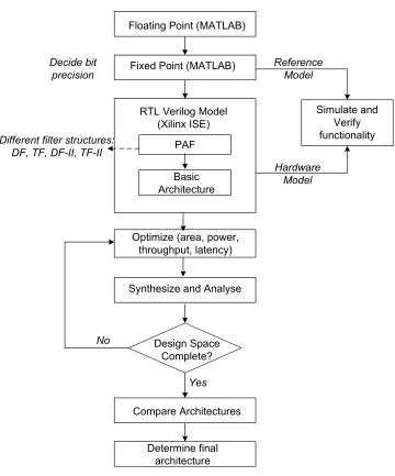
DWT. We use the design flow illustrated in Figure3.1in order to accomplish our goal.
1. Model the initial algorithm in MATLAB using floating point computations.
This model uses the same 1-D DWT architecture that was used for the basic hardware implementation suggested by Mallat [10].
2. Refine the floating point model to a behavioral fixed point model to achieve bit-wise accuracy (using MATLAB). This fixed point model can be used to generate
test sequences to validate the hardware. The fixed point model serves as a
reference for the hardware and generates the same output results as expected from the hardware implementation.
! " # $ ! % $
! $ &
& # &
' !
( "! )
( "!
' " *
" *&
* &
Figure 3.1: Design Flow
as Verilog to obtain a functionally correct hardware implementation of the 1-D DWT. This model uses two’s complement fixed point arithmetic. The
perfor-mance analysis framework (PAF) [23] assists us in deciding the different filter structures. The results obtained from the RTL design of the DWT architec-ture are simulated (using Xilinx ISE software) and compared with the results
design.
4. Apply optimization techniques to improve the hardware efficiency. The
ini-tial DWT hardware model is modified to include optimizations that improve throughput, power consumption, latency and hardware resource utilization.
5. Analyze performances of the hardware architectures in the design space and
determine an efficient architecture for the FPGA implementation. This is an incremental design and analysis process.
The tools required for the completion of this work are MATLAB and Xilinx ISE
software. MATLAB (from The Mathworks) is a high-level of technical computing
language for algorithm development [24]. It has built-in functions that can help solve technical problems more conveniently than with C or C++. MATLAB has the DWT toolbox which has the functions to generate wavelet coefficients and to compute the
DWT which assists us in developing our initial 3-level DWT algorithm faster. Xilinx
ISE allows us to implement our architecture, simulate and synthesize our design on the FPGA used for our work. The cycle-accurate RTL models are coded using Verilog,
which is the popularly used HDL for digital systems.
3.1
Floating Point Implementation
For most digital hardware systems, the coefficients, inputs, intermediate outputs
and the final outputs are stored in finite word registers using the binary number for-mat. This requires quantization of floating point values depending on the number of
bits used for precision. The representation of the IEEE single precision floating point
Figure 3.2: Single Precision IEEE floating point format
where s is the sign bit, e is the biased exponent and m is an unsigned (normalized)
mantissa. The actual exponent can be determined by [e−bias] where bias= (2E−1
−
1). For the IEEE single precision format, E is 8 bits, hence, bias is 127. A floating point number can be represented using Equation 3.1 [4].
x= (−1)s 1.m 2e−bias (3.1)
The roundoff and overflow errors associated with quantization affect the mantissa
of the floating point number. For accurate computations with floating point arith-metic, the exponents of the operands might have to be modified. For example, for
addition operations, the exponents of the two operands should have the same value.
If the exponents are not equal, they have to be adjusted such that they are lined up. Similarly, for multiplication, the mantissas are multiplied and the exponents are
added [26]. Therefore, the use of floating point arithmetic to implement hardware systems requires complex hardware, which slows down the speed of the processor and increases power dissipation [4].
Floating point implementation proves very useful in helping us conceptualize our
design. It also provides a solid base for comparing the results of the fixed point and Verilog implementations. Hence, it is worthwhile to develop the floating point
im-plementation using a high level language such as MATLAB. Lower levels of design
We begin the development of the floating point three-level 1-D DWT algorithm
in MATLAB by developing a basic DWT block as shown in Figure 2.3. The inputs to the basic DWT block function are: the input signal, the low pass filter coefficients and the high pass filter coefficients. The input signal is convolved with the low pass
and the high pass filter coefficients using the built-in MATLAB function conv. The
outputs obtained after filtering are downsampled by removing every other odd sample.
The alternate built-in MATLAB function to perform the computation for a single
level DWT block decomposition is dwt [24]. The filter coefficients are obtained from the Daubechies orthogonal family. For this thesis, we use the ’db8’ filter family for
its smooth spectral properties which make them suitable for many speech and
im-age processing algorithms [11]. Additionally, the db8 family filters are 16 tap filters which are an appropriate choice to illustrate the complexity of the DWT algorithm for higher order filters. The hardware implementations considered in this work are
applicable to other wavelet families and various filter orders. The decomposition and
reconstruction filter coefficients for the db8 wavelet family can be obtained from the MATLAB function wfilters.
A three level implementation of a 1-D DWT can be done by cascading the DWT blocks using appropriate input signals as shown in Figure 2.4. Floating point com-putations have the advantages of a large dynamic range, high resolution and
compu-tational precision, but the disadvantages of slow speed and high system complexity.
3.2
Fixed Point Implementation
Fixed point numbers have a predetermined exponent as opposed to the varying
exponent for floating point numbers. Additional logic is not required to compute the exponents which significantly speeds up the computation process. The system
hardware required for fixed point implementations is less complex which also reduces
point computations, many hardware platforms, such as the ASICs and FPGAs prefer
the use of fixed point arithmetic.
The dynamic range for N bit fixed point number is [−2N−1,2N−1−1]. The Q m.n
format is used to represent N bit fixed point numbers where the MSB bit is the sign
bit, m is the number of bits used to represent whole numbers and n =N −(m+ 1) is the number of bits used to represent fractional bits [26]. We use the Q0.n format to model the inputs, coefficient and outputs using fixed point numbers for our work.
This representation assumes that the floating point inputs and coefficients are nor-malized in the range of (-1,1). Therefore, the range of N bit fixed point numbers in
Q0.n format is [−(1−2−n),1−2−n], where n =N −1.
The twos complement representation is widely used to represent fixed point num-bers in hardware systems. A value of 2N can be added to negative numbers to obtain
their corresponding twos complement numbers. Hence, instead of negative numbers
having the range of [−2N−1
,0), the range for twos complement negative numbers is [2N −2N−1,2N). The use of twos complement format to represent numbers makes arithmetic computations relatively straightforward since it eliminates the need for a
sign bit [26].
We proceed with our design cycle by implementing the DWT algorithm using fixed
point numbers. Scaling techniques need to be applied on floating point numbers, to obtain N bit fixed point integers. The floating point input sequence is scaled using
Equation3.2to represent the fixed point numbers within the specified dynamic range.
InputSF = 2 N−1
−1
max(|x|)
xscaled = b(InputSF ∗x)c
(3.2)
Wherexis a range of input andInputSF is the factor by which the inputs are scaled.
re-sult obtained is floored or truncated to obtain its corresponding N bit fixed input
sequence xscaled. The other alternative quantization modes tof loor in MATLAB are
rounding, ceil and fix. Scaling using these quantization modes give different results, but the round mode gives most accurate results when compared with floating point
values. However, the round mode requires more complex hardware. The floor mode
is found to be the simplest quantization method to implement in hardware and is, therefore, commonly used for fixed-point representation [27].
Operations such as multiplications and additions in the filtering operation may lead to overflow of bits. For hardware systems, the intermediate outputs that result
out of these operations also require scaling or truncation. To avoid overflow caused
due to finite number of registers, the filter coefficients are scaled by using the output
overflow criterion [15] [26]. The filter coefficients b(k) are scaled using Equation 3.3.
F ilterSF = ymax
xmax∗bsum bscaled = b(F ilterSF ∗b)c
(3.3)
Where, ymax is the maximum value the output can take depending on the size of
output registers, xmax is the maximum value of the input and bsum is the sum of
the absolute values of all the filter coefficientsb(k). The value,F ilterSF is the factor by which the filter coefficients are scaled such that there is no overflow andbscaled are
the scaled filter coefficients. Therefore, the result of filtering a N bit input sample
with N bit filter coefficients is a 2N bit output sample.
3.3
Hardware Implementation
The next step in the design process is to capture a functionally correct hardware algorithm using Verilog RTL. The design is verified by comparing the results obtained
The waveforms of the MATLAB and Verilog models are plotted to verify functional
correctness.
The basic binary tree structure implementation for a 3-level, 8-channel
convolu-tion based architecture is described in Secconvolu-tion 2.2. The architecture implemented in Figure 2.4 has several design inefficiencies. These include large critical path delay for cascaded FIR filters, poor hardware utilization due to the use of redundant filters
for level 2 and higher and inefficient power dissipation due to the wastage of every
alternate computation performed at the output of the decimation filters. We address these inefficiencies through an incremental design and analysis process to improve
performance. We realize our final architecture by applying a combination of various
optimizations to the basic design to achieve good hardware utilization, reduced
criti-cal path and efficient power utilization. The following hardware performance metrics assist in analyzing the performance improvement of the hardware architecture.
3.3.1
Hardware metrics
The performance of the architecture is evaluated with respect to area, throughput,
latency and power consumption. We define the hardware performance metrics used
in our work as listed below.
1. Area
The traditional FPGA structure consists of three key elements: a two-dimensional array of logic elements, input output blocks (IOBs) and programmable
inter-connects (PIs). The logic elements in Xilinx FPGAs are called configurable
logic blocks (CLB). These CLBs are made up of look-up tables (LUT) and flip-flops and can implement both, combinational and sequential logic. The newer
generation of FPGAs, such as the one used in our work have RAM blocks and
Figure 3.3: General FPGA architecture [4]
The DSP blocks within the FPGAs are extremely effective for digital signal
processing applications and can achieve frequencies of up to 550MHz [5]. The number of logic cells, DSP blocks, CLBs, IOBs and RAM within the FPGA
vary with different FPGA families and their architecture is vendor-specific.
However, the FPGA resources are limited and should be prudently used. In order to achieve the design objective of minimum area, we focus on reducing
the number of resources consumed by mathematically intensive algorithms on
an FPGA. This enables large MAC intensive designs to fit within the chosen
FPGA.
2. Throughput
!" #$ % & '(
Figure 3.4: Critical Path Delay
The time taken for a signal to pass through the critical path determines the operational clock frequency and hence the throughput of the system. We
define throughput as the number of samples obtained in one second, for our
work.
3. Hardware Latency
Latency is the time taken by a signal to pass through a system. It is the
time difference when the input is applied and when the corresponding output
is obtained. Figure 3.5 illustrates an example of the latency. In Figure 3.5 we
Figure 3.5: Latency
the corresponding output signal is obtained at the output at t= 5. Hence the
latency is 2 clock cycles.
4. Power
The power consumptionof an FPGA is a critical design constraint for small
hardware platforms such as portable electronics which have limited battery
life [4]. We analyze power based on the number of computations within the system and the dynamic power dissipated during the switching associated with
these computations.
3.3.2
Filter structures
The SFG of the basic architecture as shown in Figure 2.4 can be implemented by using identical filter structures for the low-pass and high-pass signal decomposition.
The transfer function for a FIR filter system in the z domain is shown in Equation
3.4.
H(z) = M−1
X
k=0
bkz−k (3.4)
where
H(z) = Output sequence Y(z)
Input sequence X(z)
Variables b(k) andM in Equation 3.4 are the filter coefficients and the filter length respectively.
This transfer function has a variety of realization structures. The FIR filters used in the DWT architecture can be implemented by using any of the conventional
fil-ter structures shown in Figure 3.6. The block diagrams in Figure 3.6 are cascaded realizations of an FIR filter of order M = 5. We observe that the filter blocks are modular in nature with regular data flow and can be easily extended to any order
Figure 3.6: Block Diagrams for FIR Structures
filter may vary depending on the choice of filter structures.
The first step towards the hardware implementation of the DWT algorithm was
Table 3.1: Comparison of different Filter Architectures
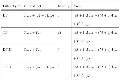
Filter Type Critical Path Latency Area
DF Tmult+ (M + 1)Tadd 0 (M + 1)Amult+ (M + 1)Aadd
+M AregN
TF Tmult+Tadd M (M + 1)Amult+ (M + 1)Aadd
+M Areg2N
DF-II Tmult+Tadd 0 (M + 1)Amult+ (M + 1)Aadd
+M Areg2N
TF-II Tmult+ (M + 1)Tadd 0 (M + 1)Amult+ (M + 1)Aadd
+M AregN
Analysis Framework (PAF) [23] provided a starting point for the implementation of the DWT. It gave an estimate of the latency, throughput and the area utilized by the
filter which assisted us in the selection and analysis process. The choices for cascaded filter blocks generated by the framework are: direct form (DF) filter, transpose (TF)
form filter, direct form-II (DF-II) and transpose form-II (TF-II).
Table 3.1 gives an approximate idea of the critical path delay, latency and the area associated with M order filter structures. There is some latency inherent in
FIR filters due to the design of the filter coefficients, however we have not included that in Table 3.1. We assume Tmult,Tadd and Treg are the times in ns required by a signal to pass through the multiplier, adder and the delay unit respectively. Amult
and Aadd are the area occupied by the multiplier and the adder respectively. We use
the notationsregN and reg2N to represent the registers occupied byN bits and 2N
The TF and DF-II filters have low critical path delays but have the problem of
data-broadcasing. DF filters have low latency but a large critical path delay. TF-II
filters also have low latency but large critical path delay. For our work, we use the DF and TF-II structures. We choose DF filters to get an assessment of the performance
improvement over Baganne’s architecture [13]. We have implemented the TF-II filter to illustrate that the choice of filters can affect the performance of the hardware. The PAF gives us the flexibility to implement different filter architectures with ease.
3.3.3
Introduction to Hardware Optimization Techniques
Optimizations are based on the technology on which the design is synthesized and the tools that can help improve the hardware utilization and reduce the powerdissipated. However, optimizations at the architectural level can significantly impact
the hardware performance of the algorithm. This section lists the commonly used hardware optimization techniques applied to DSP hardware algorithms.
Polyphase
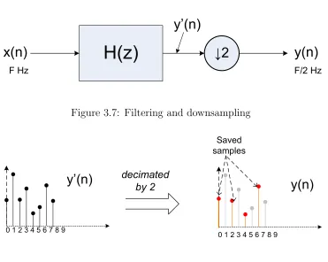
Multirate DSP systems are commonly used in many practical signal processing
applications that require different sampling rates. Downsampling and Upsampling are common techniques used for sampling rate conversion in analysis and synthesis
filters such as the QMF banks [30]. The input is filtered and downsampled by a factor of two at every stage of the DWT algorithm. Downsampling, also known as
decimation, can be easily implemented as shown in Figure 3.7.
whereH(z) is the filter transfer function, x(n) is the input signal,y0(n) is the filtered
output and y(n) is the final decimated output signal. The input clock frequency is F Hz and the output clock frequency is F/2 Hz. Figure3.7illustrates a sample waveform for the output sequence after filteringy0(n) and the output sequence after decimation
y(n).
Figure 3.7: Filtering and downsampling
Figure 3.8: Example of decimation by 2
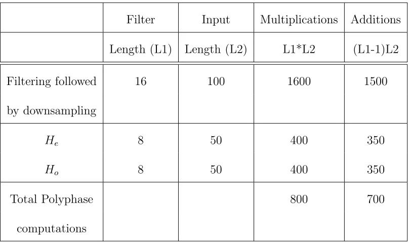
wastage of computations can be avoided by using two-phase polyphase filters as shown
in Figure 3.9. The polyphase technique is widely used in multi-rate high speed filters
Figure 3.9: Polyphase structure
Table 3.2: Comparison of computations for polyphase and non-polyphase filters
Filter Input Multiplications Additions
Length (L1) Length (L2) L1*L2 (L1-1)L2
Filtering followed 16 100 1600 1500
by downsampling
He 8 50 400 350
Ho 8 50 400 350
Total Polyphase 800 700
computations
H(z) =b(0)z0
+b(1)z−1
+b(2)z−2
+b(3)z−3
+b(4)z−4
+b(5)z−5
(3.5)
The above filter can be split into its corresponding polyphase filters as shown below:
Heven(z) = b(0) +b(2)z−2
+b(4)z−4
Hodd(z) = z−1
(b(1) +b(3)z−2
+b(5)z−4 )
where
H(z) =Heven+z−1Hodd (3.6)
The advantage of this method is that the same functionality can be achieved by computing only the necessary values. This avoids wastage of computations which in
turn reduces the power dissipated. In case of DF filters, the critical path through the
filter is also reduced since the filter is divided into two filters for decimation by 2. In
Table 3.2 shows the number of multiplications for polyphase and non-polyphase structures. The table shows there is a saving of half the multiplications and more
than half of the additions. We confirm that the use of polyphase technique for down-sampling filters allows calculation of only the values to be saved which reduces the
number of computations. Hence, the power dissipated by decimation filters that
use the polyphase technique is less than that for those that do not use polyphase implementation.
Pipelining
The pipelining technique is used in hardware systems for concurrent processing.
Concurrent processing of data divides the computational load between multiple
pro-cessing elements which in turn helps achieve high propro-cessing rates for large designs. Pipelining techniques can reduce the critical path delay of the system and can
elim-inate broadcasting and global interconnections within the design. There are two
techniques used to pipeline the design: the interleaving technique and the delay technique [31]. The techniques developed by Dabbagh et al. are based on the prop-erties of thez-transform and can be applied to modular structures such as the digital
FIR filter used in our design. We briefly review these techniques and apply them to our design.
• Interleaving Technique
Interleaving can be achieved by replacing the unit time, z−1
in a system with
z−k, where k is a positive integer. The interleaving technique is illustrated in Figure 3.10. Figure3.10 illustrates a filter system before and after interleaving. In the top system H(z) is the filter transfer function, X(z) is the input signal and Y(z) is the output signal without any interleaving. Figure 3.10 shows ak
interleaved filter system, where H(zk) is the filter transfer function, X(zk) is
the input signal and Y(zk) is the output signal. The effect of interleaving is
Figure 3.10: Filter zero-interleaved by factor ’k’
extra delays can be distributed within the system to achieve pipelining.
• Delay Technique
The delay technique delays the output of the system by multiples of the unit time delay. Usually this delay is equal to the order of the filter for a FIR filter.
These delays can be distributed uniformly within the system and can reduce the
critical path of the design. For a DF FIR filter, the delays can linearly speed
up the design at the cost of increased hardware latency.
Pipelining techniques can help reduce the critical path, eliminate broadcasting
and global interconnections. However, these techniques need to be applied carefully to ensure the timing of the system is retained. One systematic way of applying these
optimizations and retain the design timing is called cut-set retiming [32]. Cut-set retiminggives a set of guidelines to be followed while applying pipelining techniques
within the design.
1. If a unit delay is added to the left arc we cut through the design and add a unit delay to all the left arcs and remove a delay from all the right arcs.
2. If there is no corresponding delay in the right arc to remove, we zero interleave
interleaving, we add delay on the right arc and remove one corresponding delay
in the left arc.
A similar procedure is followed if a delay is added to the right arc. For DSP designs we prefer the data flow in one direction since the data flow in multiple directions
could lead to tighter constraints on the timing and will slow down the clock. Figure
3.16 and Figure 3.17 illustrate how cut-set retiming is applied on DF and TF-II FIR filters.
Data-Interleaving
The two optimization techniques suggested above, namely polyphase and
pipelin-ing can be applied to the DWT algorithm within each DWT block. The pipelinpipelin-ing
technique can also be applied to the system between each stage to speed up the design and reduce the critical path delay of the entire system. In this section we elaborate
on the data-interleaving technique used in our design.
Data-interleaving helps process multiple independent signals using a single filter
structure. If two signals are filtered independently by identical filters, we can use
only one filter instead of two, interleave the inputs and add delays to the system. Figure 3.11(a) illustrates two different input sequences, x1(n) and x2(n) are filtered by identical filters H(z). The output sequences are y1(n) and y2(n) respectively.
We can zero-interleave the filter by a factor k = 2 for two signals by using the
method described in pipelining section above. We could zero-interleave the filter by
a factor k = n for n independent signals. The two input signals are interleaved and filtered as shown in Figure3.11(b). Though interleaving by a factork= 2 will double the registers in the filter, it will use the same number of multipliers and adders as
(a) Two independent signals filtered by two identical
filters
(b) Interleaved signals filtered by single filter interleaved byk= 2
the input signals independently.
These kinds of optimizations can help reduce the resource utilization for a de-sign that has similar filters for input de-signals. This results in a considerable
sav-ings in resources and efficient hardware utilization. However, interleaving a cascaded
non-polyphase filter will reduce the throughput of the design, but if interleaving is combined with polyphase filters, it will maintain the throughput and also reduce the
resource consumption. This is explained in Section3.4.4. Therefore, data-interleaving technique encourages resource sharing and efficiently utilizes the hardware.
3.4
Hardware Design Implementation
3.4.1
Basic Implementation
The basic implementation of a 3-level 8-channel convolution based 1-D DWT
al-gorithm is described in Chapter2. The filter blocks are cascaded as shown in Figure
2.4. Further details of the inputs and outputs of each level and their frequency range is given in Section 2.2.1. Figure 3.12illustrates the behavior of the input and output sequences for each level of decomposition. The length of the input and output samples
have to be retained irrespective of the optimizations to maintain correct functionality
of the DWT algorithm. In Figure3.12, we show only one of the outputs of every level for illustration purposes. All the other outputs for a particular level of
implementa-tion are equivalent in length to the one illustrated.
The filtered output obtained at each level is downsampled by a factor of 2 as
shown in Figure2.4. The number of decimated output samples is half the number of input samples for each level since every even sample is retained and every odd sample discarded. The waveforms for level 1 downsampled output are shown in Figure 3.13. The control signaldownsampler for level 1, is held high for alternate clock cycles. The
Figure 3.12: IO waveforms for a DWT algorithm
high, the filtered output is sampled and the time when the downsampler is low the filtered output is discarded. Similar downsampling logic is implemented for higher
levels of decomposition, where for level J implementation the downsampler toggles
every 2Jth clock edge.
! "
#!#!
Figure 3.13: Decimation by two
The critical path delay for an Mth order DF FIR filter for a 3-level
implementa-tion is (Tmult+ 3 (M+ 1)Tadd), which is undesirably large. The basic implementation
![Figure 3.3: General FPGA architecture [4]](https://thumb-us.123doks.com/thumbv2/123dok_us/1396351.1172338/43.612.188.464.121.328/figure-general-fpga-architecture.webp)