University of South Carolina
Scholar Commons
Theses and Dissertations
1-1-2013
III-V Nitride Micro- and Nano-Scale Cantilevers
For Multimodal Sensing Applications
Ehtesham Bin Quddus University of South Carolina
Follow this and additional works at:https://scholarcommons.sc.edu/etd Part of theElectrical and Electronics Commons
This Open Access Dissertation is brought to you by Scholar Commons. It has been accepted for inclusion in Theses and Dissertations by an authorized administrator of Scholar Commons. For more information, please [email protected].
Recommended Citation
III-V
NITRIDE MICRO-
AND NANO-
SCALE CANTILEVERSFOR
MULTIMODAL SENSING APPLICATIONS
by
Ehtesham B. Quddus
Bachelor of Science
Bangladesh University of Engineering and Technology, Dhaka, Bangladesh, 2006
Submitted in Partial Fulfillment of the Requirements
For the Degree of Doctor of Philosophy in
Electrical Engineering
College of Engineering and Computing
University of South Carolina
2013
Accepted by:
Goutam Koley, Major Professor
Tangali S. Sudarshan, Committee Member
Grigory Simin, Committee Member
Richard Webb, Committee Member
© Copyright by Ehtesham B. Quddus, 2013
DEDICATION
To my parents,
To my lively wife Shakila,
ACKNOWLEDGEMENTS
I would like to thank my Supervisor Dr. Goutam Koley for supporting me during
these five years. Working with Dr. Koley, in my opinion, is the best thing that a PhD
student can wish for. He perfectly translates the character of his students and provides the
best conditions for the development of intellectual qualities and creative thinking. I am
very grateful to him for his scientific advice and knowledge and many insightful
discussions and suggestions he provided me and beyond all his guidance in my tough
times.
I owe my gratitude to all of the dissertation defense committee members,
Professor Richard Webb, Professor Sudarshan and Professor Simin for their career advice
and suggestions in general.
I will forever be thankful to Professor Webb not only to let me use his facility
(Low Temperature and Mesoscopic Physics Laboratory aka Dr. Webb’s Lab) located at
the Nanocenter but also he has been very helpful in providing advice many times during
my PhD. In particular, I would like to express my gratitude to Prof. Webb for his support
in the nanoscale characterization and device fabrication using his lab facilities. He is one
of the smartest people I know; I hope I could be as lively, enthusiastic, and energetic as
I also thank to Professor Sudarshan and his Silicon Carbide Lab, particularly in
helping me to use the leak detector for my CVD furnace and also letting me use the
Cleanroom facility. Part of the NEMS fabrication processes were done at his cleanroom.
The Microfabrication part was done using the class 10/ class 100 cleanroom
facilities at the IEN at GaTech. I have been visiting to GaTech since March 2011 and met
really nice people and stuff there. They showed me light in the tunnel many times while I
was stuck with the complex processes, I owe my gratitude to all of the stuff members of
MiRC and IEN who have made this research possible, especially for their personal and
technical support.
This work has been done in collaboration with Oakridge National Lab (ORNL)
and National Institute of Standards and Technology (NIST). I would like to thank Dr.
Karren More at the ShaRE facility at Oak ridge and Prof. Steve Semancik at the NIST for
letting me use their state of the art equipments.
I would like to acknowledge the financial support from NSF grant that funded
part of the research for this dissertation.
I thank to all the present members of Dr. Koley’s group. Special thanks to Amol
Singh for guiding me as a senior member, Alina Wilson for helping me last two and half
years with Nanowire growth and characterization and also Nick De Roller for providing
me the COMSOL simulation results. My research for this dissertation would not have
been successful also without the efforts of all the past colleagues in our research group;
Qazi, Dr. Jie Lie, Dr. Waliullah Khan Nomani, Mr. Devendra Diwan and Mr. Stephen
Orr.
Finally, my long tenure as a graduate student would not have been possible without
the support and patience of my family. I wish to express my heartfelt gratitude to my
parents and also I am deeply indebted to my beloved wife Shakila Afrin; their love and
ABSTRACT
Recent research trends in chemical and biological sensing have been geared
toward developing molecular sensor devices that are fast, label free, miniaturized and
portable. The performance of these devices can be dramatically improved by utilizing
multimodal detection techniques, new materials and micro-/nanofabrication technologies.
This is especially true for micro-/nanoscale cantilever sensors, which undergo changes in
mechanical or electrical properties upon the specific binding of molecules. To develop
the sensor devices with the above attributes, we utilized III-V nitride materials: InN
nanowires for realizing nanoscale cantilevers and AlGaN/GaN heterostuctures with or
without embedded HFETs, for developing microcantilevers. There are mainly two
approaches of fabricating these sensor devices: bottom-up approach for nanocantilevers,
and top-down approach for microcantilevers. InN NWs, which exhibit interesting
properties such as high carrier density, superior electron mobility, strong surface charge
accumulation, and chemical inertness, were synthesized using Chemical Vapor
Deposition (CVD) technique by Vapor-Liquid-Solid (VLS) mechanism. The synthesis
process was optimized to obtain growth direction modulation and enhanced performance
of the devices, largely avoiding the complexity of nanofabrication/ etching typically
involved in the realization of nanoscale sensors. With dimensions much smaller than
and piezoelectric properties of AlGaN/GaN heterostructures, their wide bandgap, and
chemical inertness make the microcantilevers very attractive for developing highly
sensitive sensors suitable for harsh environment applications. The large variation in
2-dimensional electron gas (2DEG) at the interface with mechanical strain makes these
microcantilevers much more sensitive than conventional Si based piezoresistive
microcantilevers. A process was developed to fabricate free standing AlGaN/GaN
microcantilevers on Si(111) substrate using various processing steps involving
photolithography, GaN and through wafer Si etching, and dielectric and metal deposition.
The detection performance of these cantilevers is largely improved by the utilization of a
TABLE OF
CONTENTS
DEDICATION... iii
ACKNOWLEDGEMENTS ... iv
ABSTRACT ... vii
LIST OF TABLES ... xiii
LIST OF FIGURES ... xiv
CHAPTER 1AIM OF DISSERTATION ... 1
1.1 Project scope ... 2
1.2 The research partners ... 2
1.3 Dissertation Aim ... 3
1.4 Outline of the dissertation ... 3
CHAPTER 2INTRODUCTION & MOTIVATION ... 6
2.1 Introduction ... 7
2.2 Chemical sensor arrays ... 9
CHAPTER 3CANTILEVER SENSORS ... 24
3.1 Cantilever sensors ... 25
3.2 Cantilever theory of operation ... 30
3.3 Modalities of Cantilever Deflection- and Vibration- Based Sensing ... 39
CHAPTER 4INDIUM NITRIDE NANOWIRES ... 59
4.1 Introduction and background ... 60
4.2 Semiconductor nanowires ... 60
4.3 Indium Nitride (InN) nanowires ... 62
4.4 Indium Nitride Nanowire synthesis ... 70
4.5 Growth optimization: Role of oxygen in the synthesis ... 77
4.6 Growth direction modulation ... 84
4.7 Electrical Characterization and Diameter-dependent mobility ... 86
CHAPTER 5INDIUM NITRIDE NANOCANTILEVERS ... 98
5.1 Introduction ... 99
5.2 InN Suspended nanostructures ... 102
5.3 Fabrication of InN NEMS resonators ... 102
5.4 DC characteristics of InN NEMS resonator ... 107
5.5 Optimization of the release process of suspended Nanostructures ... 109
5.7 InN Nanowire Based V-shaped Cantilever Sensors ... 118
5.8 Fabrication steps of InN nanocantilever sensors ... 136
CHAPTER 6ALGAN/GAN HETEROSTRUCTURES ... 140
6.1 Introduction ... 141
6.2 Gallium Nitride crystal structure ... 144
6.3 Spontaneous and piezoelectric polarization ... 145
6.4 Growth of AlGaN/GaN heterostructures ... 149
6.5 Formation of 2DEG ... 152
CHAPTER 7ALGAN/GAN MICROCANTILVERS ... 160
7.1 Introduction ... 161
7.2 HFET embedded V-shaped AlGaN/GaN microcantilever ... 162
7.3 V-shaped AlGaN/GaN micro heater cantilever ... 175
7.4 Fabrication of AlGaN/GaN V-shaped microcantilevers ... 184
7.5 Measurements of AlGaN/GaN Microcantilevers ... 199
CHAPTER 8CONCLUSION AND FUTURE PLAN ... 225
8.1 Summary ... 226
8.2 Future work ... 227
LIST
OF
TABLES
Table 4.1 Lattice parameters of wurtzite III-V nitrides at 300 K. ... 65
Table 4.2 Effects of lattice non-ideality on the strength of spontaneous polarization in the III-V nitrides. ... 67
Table 5.1 Simulated material constants ... 121
Table 5.2 Simulated Model Properties... 121
Table 6.1 Electronic properties of some common semiconductors, Ref. [241] ... 142
Table 6.2 Structural parameters for AlN, GaN, and InN. ... 145
Table 6.3 The dependence of spontaneous polarization on the c0/a0 ratio, Ref. [243] ... 146
Table 6.4 List of elastic and piezoelectric constants used for calculation ... 148
Table 7.1 Dimension of the AlGaN/GaN HFET embedded microcantilevers and calculated k and f. ... 164
Table 7.2 Dimension of the AlGaN/GaN HFET ... 164
Table 7.3 Properties of GaN and AlGaN used for COMSOL simulations ([Ref. 253]) . 170 Table 7.4 Calculated parameters from the TLM test ... 201
LIST
OF
FIGURES
Figure 2.1: Various applications of chemical sensors ... 15
Figure 3.1: Two modes of cantilever-based biomolecule detection: (a) deflection mode and (b) resonance mode. ... 31
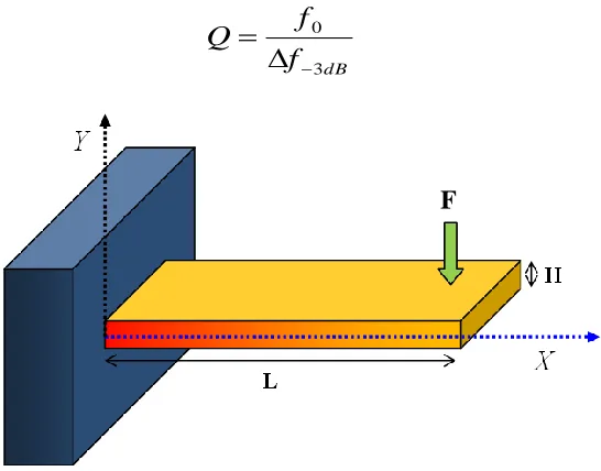
Figure 3.2: Schematic of a cantilever with length L and thickness H, with respect to coordinates X and Y, before being deflected by a point force F applied on the tip. ... 34
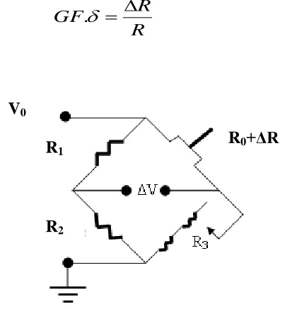
Figure 3.3: Schematic diagram of a microcantilever with embedded piezoresistive transduction element embedded at the base of the cantilever. ... 40
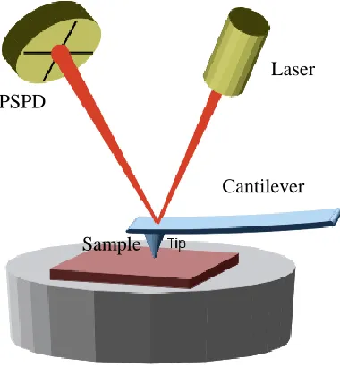
Figure 3.4: Simplified schematic diagram of optical transduction system used in atomic force microscope. ... 41
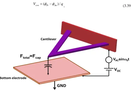
Figure 3.5: Simplified schematic diagram of capacitive transduction system of a microcantilever based sensor. Due to adsorption on the functionalizing layer the cantilever bends, changing the capacitance between the two conducting plates ... 43
Figure 3.6: Schematic of the interaction between probe and target molecules on an embedded-MOSFETcantilever system. The silicon nitride cantilever is a reference, and the gold-coated one is used as a sensing cantilever. Specific biomolecular interactions between receptor and target bend the cantilever. Magnified view of embedded MOSFET in cross section shows stressed gate region when cantilever bends, resulting in change of drain current due to conductivity modulation of the channel underneath the gate.(Figure taken from Ref [137]) ... 44
Figure 3.7: Resistance of a heated cantilever as a function of power dissipation and illustration of heat transfer by heated cantilevers since they are very sensitive to small thermal agitation (Ref [153]). ... 46
Figure 3.8: (a) the adsorption and (b) the absorption mechanism of molecules on cantilever surfaces ... 48
protonation/deprotonation equilibria that change the surface charge state with pH. (d) Conductance of an unmodified Si nanowire device (red) versus pH. The dashed green curve is a plot of the surface charge density for silanol groups on silica as a function of pH (Ref. [157])... 51
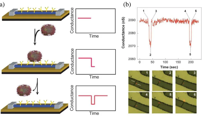
Figure 3.10: (a) Schematic of a single virus binding and unbinding to the surface of a Si nanowire device modified with antibody receptors and the corresponding time-dependent change in conductance. (b) Simultaneous conductance and optical data recorded for a Si nanowire device after the introduction of influenza A solution. The images correspond to the two binding/unbinding events highlighted by time points 1-3 and 4-6 in the conductance data, with the virus appearing as a red dot in the images (Ref. [158]). ... 52
Figure 3.11: Physics of potentiometric measurement with a cantilever oscillating above substrate. ... 55
Figure 3.12: Band diagram illustrating Fermi level and vacuum level for Si cantilever probe and semiconductor substrate. ... 57
Figure 4.1:Density of states in semiconductor structures depending on dimensionality (Ref. [120]). ... 62
Figure 4.2: Atomic arrangements in In-face and N-face InN crystals. The red arrow pointing from N to In atom shows the direction of the spontaneous polarization (Ref. [184])... 64
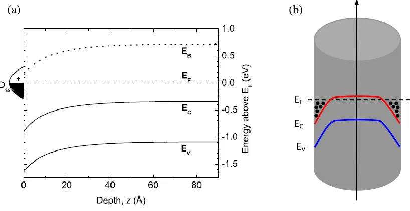
Figure 4.3: The conduction and valence band edges (EC and EV, solid lines) and the
branch-point energy (EB, dotted line) with respect to the Fermi level (EF, dashed line) in
the near-surface region of InN(0001). The donor-type surface states (Dss) are also shown, where the unoccupied states above the Fermi level are shown to be positively charged. 69
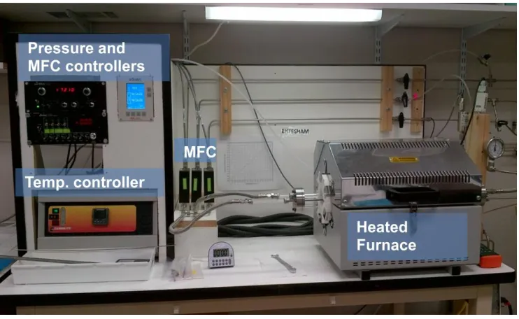
Figure 4.4: CVD system setup, Pressure and MFC controllers, MFCs, Temperature controllers and heated furnace ... 71
Figure 4.5: (a) A typical SEM image of InN nanowires as-synthesized on a Si/SiO2 substrate. Inset shows a single NW, scale bar is 20 nm. (b) High resolution TEM image of a single NW growing along [110] direction, the inset shows the hexagonal FFT spectrum. (c) Atomic resolution shows the lattice spacing of the NW. ... 72
Figure 4.6: Energy Dispersive Spectroscopy (EDS) mapping on section of a nanonetwork. (a) STEM Image. (b) In elemental mapping, (c) N elemental mapping and (d) O elemental mapping along the nanonetwork. ... 74
Figure 4.7: NWs growing on a 40 nm thick SiO2 membrane from catalyst patterns outside the membrane (Si support). ... 75
Figure 4.9: The morphologies obtained at different oxygen (3% in balance N2) flow rates in sccm: (a) 0 sccm; (b) 2.0 sccm; (c) 4.0 sccm; (d) 8.0 sccm; (e) 10.0 sccm; (f) 14.0 sccm. ... 80
Figure 4.10: HTREM images of single NWs at different oxygen (3% in balance N2) flow rates in sccm a) 2 sccm; (b) 4.0 sccm; (c) 10.0 sccm; (d) 14.0 sccm. Insets show the hexagonal FFT spectra respectively. ... 82
Figure 4.11: Energy Dispersive Spectroscopy (EDS) mapping on section of a nanowire. (a) STEM Image. (b) In elemental mapping, (c) N elemental mapping and (d) O elemental mapping along the nanowire for 4 sccm of O2 concentration. ... 83
Figure 4.12: Energy Dispersive Spectroscopy (EDS) mapping on section of a nanonetwork. (a) STEM Image. (b) In elemental mapping, (c) N elemental mapping and (d) O elemental mapping along the nanonetwork for 10 sccm of O2 concentration. ... 84
Figure 4.13: SEM images showing (a) spontaneous bending of InN NW, as well as bending caused by (b) two InN NW guides (c) lithographically deposited 100 nm SiO2 barriers and (d) Lattice resolved TEM images of a NW showing atomic arrangement as the growth direction is changed from [110] to another [110], inset shows schematic diagram of atomic configurations for 60° (similar to 120°) bend... 86
Figure 4.14: (a) SEM image of a 3 NW FET in a back-gated configuration. (b) Id-Vd curves for the InN NW FET at gate bias voltages between 0 V to 3.6 V at intervals of -0.4 V. (c) An Id-Vg curve measured at Vd = 0.2 V, with the dId/dVg slope shown by a straight line. (d) Id-Vd saturation curves measured for gate bias voltages between 0 V and
-4.0 V at intervals of -0.5 V. ... 88
Figure 4.15: Variation of (a) mobility and (b) conductivity of InN NWs as a function of the diameter obtained from single and multi-NW FETs. The respective error bars are also shown. Inset of (b) shows the variation in carrier concentration with NW diameter. ... 92
Figure 4.16: Variation of (a) mobility and (b) conductivity of InN NWs as a function of NW diameter fitted with diameter-dependant mobility and conductivity obtained from theoretical modeling (solid lines). Inset of (b) shows the variation of mobility with carrier concentration. ... 96
Figure 5.1: A typical example of a silicon nanowire based NEMS resonator (Ref. [224]). ... 99
Figure 5.2: Plots showing the number of yearly peer reviewed publications as obtained from Web of Search with a key “nanocantilever” and “nanocantilever sensor”. ... 100
Figure 5.3: Wafer information for the processing of InN NEMS resonators ... 103
Figure 5.6: (a) Schematic representation and (b) SEM image of 2 nm thick, 2um diameter catalyst spots ... 105
Figure 5.7: (a) Schematic representation and (b) SEM image of NWs grown from catalyst spot ... 105
Figure 5.8: (a) Schematic representation and (b) SEM image of NW and etched trench106
Figure 5.9: (a) Schematic representation and (b) SEM image of NW, trench and probe contact ... 107
Figure 5.10: The dc characteristics curves for InN nanoresonators, (a) before trench etching and (b) after trench etching. ... 108
Figure 5.11: Id – Vg characteristics of InN NEMS resonator, from this curve we calculated
the mobility of the InN NW. ... 109
Figure 5.12: The schematic representation of the final NEMS resonator, NWs should be going across the trench with no sagging. ... 110
Figure 5.13: SEM images of InN NWs on the trenches, both cases the NWs fell down inside the trench. ... 110
Figure 5.14: SEM image of an InN NW across a trench, the trench was etched by Inductively Coupled Plasma (ICP) dry etch recipe... 112
Figure 5.15: (a) Image of a Dual beam FIB, (b) Inside of the dual beam FIB and schematics of different components of a dual beam FIB ... 113
Figure 5.16: The schematic representation of the final NEMS resonator with FIB; NWs are going across the trench with no sagging and the probe contacts are not solid filled 114
Figure 5.17: (a) SEM image of a pre-growth trench and (b) the SEM image of a pre growth trench and 2nm thick catalyst spots ... 115
Figure 5.18: SEM image of a pre growth trench and a suspended NW crossing across the trench... 116
Figure 5.19: Image of the designing of contact pads via FIB software ... 116
Figure 5.20: (a) SEM image of a suspended NW and the patterned and deposited FIB traces, (b) SEM image (close view) of another suspended NW, the etched profile can be seen as a measure to disconnect or cut down the NW from conducting through other NWs. ... 117
the wire bonded contact pads and (d) image of the final 40 pin DIP Chip containing active devices. ... 118
Figure 5.22: Three-dimensional model used to perform analyses. ... 121
Figure 5.23: System quality factor (QT) as a function of ambient air pressure. After about
200 Pa, damping is predominantly determined by squeeze-film losses. ... 125
Figure 5.24: Frequency sweep output of the model structure. Displacement is measured at the cantilever tip. ... 126
Figure 5.25: Sensing configuration for the VNC sensor... 128
Figure 5.26: Fundamental resonant frequency change given a mass attachment at the cantilever tip. The inset shows greater detail in the 10-23 g decade mass range. ... 129
Figure 5.27: Capacitance (blue) plotted against the bias applied to the cantilever. Deflection (green) is also present to compare with the device deflection limitation (red) of the dielectric strength of air breakdown point (3×10⁶ V/m). ... 130
Figure 5.28: Resistance change from displacement. The charged cantilever, when subjected to bending (induced or through capacitive force) will exhibit a change in charge, which may be translated into a change in resistance. ... 131
Figure 5.29: Temperature and current response across a small range of input voltages. 132
Figure 5.30: (a) Scaled (by 190) increase in length of the VNC due to temperature rise caused by an applied bias of 850 mV, and (b) displacement across a range of temperatures given by an applied voltage. ... 133
Figure 5.31: (a) SEM image of a V-shaped NW deflected back and forth by oxide barriers and (b) SEM image of a suspended NW across the trench. ... 135
Figure 5.32: The fabrication process flow of V-shaped nanocantilevers. ... 136
Figure 5.33: SEM image of 200nm thick SiO2 barriers and (b) SEM image of a V-shaped
NW deflected back and forth by SiO2 barriers ... 137
Figure 5.34: SEM image of a V-shaped NW device, the etching of the underneath SiO2 is
not performed yet (not V-shaped nanocantilever). The contacts are seen in the SEM image. ... 138
Figure 6.1: Bandgap of common semiconductors at room temperature plotted against their lattice constant, Ref. [241]. ... 141
Figure 6.3: Atomic arrangement in Ga-face and N-face GaN crystals. The arrow pointing from N to Ga atom shows the direction of the spontaneous polarization. ... 144
Figure 6.4: The direction of piezoelectric polarization with (a) compressive, and (b) tensile stress on Al(/Ga/In)N layer. ... 147
Figure 6.5: Typical layer structures of nitride heterostructures grown by MOCVD. ... 150
Figure 6.6: Layer structures of Ga-face and N-face nitride heterostructures grown by MBE on sapphire. Note that the N-face structure does not have a nucleation layer (a low temperature GaN nucleation layer can also be used to get N-face polarity). ... 152
Figure 6.7: Variation of the spontaneous and piezoelectric polarization of AlxGa1-xN and
the bound charge at AlGaN/GaN interface plotted against aluminum mole fraction of AlxGa1-xN [245]. ... 155
Figure 6.8: Conduction band diagram, sheet charge densities at the surface and interface of AlGaN/GaN heterostructure. ... 156
Figure 6.9: Sheet carrier concentration of the 2DEG confined at a Ga-face (GaN/AlGaN/GaN) or N-face (GaN/AlGaN/GaN) interface for different thickness of the AlGaN barrier. The insert shows the maximum sheet carrier concentration of a pseudomorphic grown Ga-face AlGaN/GaN and a N-face GaN/AlGaN heterostructure. ... 158
Figure 7.1: Schematic diagram of the AlGaN/GaN HFET embedded V-shaped microcantilever. ... 163
Figure 7.2: (a) Geometrical parameters of a triangular cantilever, (b) Calculation of
moment of cross-sectional area, I for one rectangular arm of a V-shaped cantilever. ... 166
Figure 7.3: Structure of a general V-shaped microcantilever. ... 168
Figure 7.4: The model used for COMSOL simulation for the AlGaN/GaN HFET embedded V-shaped microcantilever ... 169
Figure 7.5: Cross section of a HFET embedded AlGaN/GaN V-shaped microcantilever showing different metal stacks (not drawn to scale). ... 171
Figure 7.6: (a) The model used for COMSOL simulation for the AlGaN/GaN HFET embedded V-shaped microcantilever, the position of the applied force of 1 nN is shown by arrow and (b) the deflection result with the applied force. ... 173
Figure 7.8: (a) scanning electron microscope (SEM) and (b) infrared (IR) microscope images of the fabricated heated cantilever, indicating heating only near the free end of the
cantilever [277]. ... 176
Figure 7.9: Design of the tapered V-shaped AlGaN/GaN microcantilevers (a) the GaN and AlGaN layer, (b) dimensions of the cantilever and (c) tapered tip dimension from the AutoCad design ... 178
Figure 7.10: COMSOL simulated frequency response of the heated microcantilever. .. 179
Figure 7.11: (a) The model used for COMSOL simulation for the tapered V-shaped AlGaN/GaN heated microcantilever, the position of the applied force of 1 nN is shown by arrow and (b) the deflection result with the applied force. ... 180
Figure 7.12: The x-direction strain distribution on the surface of the cantilever. Insets show expanded view of the base area. ... 181
Figure 7.13: (a) Temperature dependence of the Raman frequency for the active E2 mode in GaN still attached to the substrates (Δ) and free-standing GaN (Ο) respectively. (b) Temperature dependence of the Raman frequency for the active A1(LO) mode in GaN still attached to the substrates (Δ) and free standing GaN (Ο), respectively. The solid curves give the best fitting using Eq. 7.06. ... 184
Figure 7.14: Layer information and spec of the AlGaN/GaN wafer. ... 185
Figure 7.15: (a) View of the complete mask (4” by 4”) with various photolithographic layers. (b) View of the all lithography layers of mask superimposed into one single area equal to the sample size of 1.4 cm by 1.4 cm. (c) Partial view of the single V-shaped HFET embedded microcantievers device. (d) Partial view of the single tapered V-shaped heated microcantilevers. ... 187
Figure 7.16: Schematic diagram and optical images for MESA Etching. ... 188
Figure 7.17: Schematic diagram and optical images for top cantilever outlining. ... 190
Figure 7.18: Schematic diagram and optical images for Ohmic contact deposition. ... 191
Figure 7.19: Schematic diagram and optical image for Schottky Contacts (HFET embedded catilever). ... 192
Figure 7.20: Schematic diagram and optical image for probe contact. ... 193
Figure 7.21: Schematic diagram and optical images for back pocket etching. ... 194
Figure 7.22: Basics of ICP Bosch process including a passivation and etching step. .... 195
Figure 7.24: Scanning Electron Microscopy images of fabricated AlGaN/GaN V shaped microcantilevers. (a) shows the tip of HFET embedded cantilever, whereas (b) the tapered shaped tip of the heated cantilever, (c) shows the HFET in one arm of the HFET embedded V cantilever, (d) the base of the heated cantilever and ohmic contact, (e) HFET embedded suspended V shaped cantilever and (f) suspended heated cantilever after through wafer etching. ... 197
Figure 7.25: TLM contact pads, before annealing and after annealing ... 200
Figure 7.26: The total resistance between contacts as a function of distance... 200
Figure 7.27: Current flow of HFET embedded (a) V-shaped and (b) rectangular cantilever ... 201
Figure 7.28: (a) Optical micrograph image of fabricated AlGaN/GaN HFET embedded V shaped microcantilever, (b) SEM image of fabricated AlGaN/GaN HFET in one arm of the V cantilever. (c) Optical micrograph image of the HFET embedded rectangular microcantilever, and (d) the SEM image of the rectangular cantilever.. ... 2032
Figure 7.29: (a), (c), (d) and (b), (d), (f) SEM images, family of curves and Id-Vg plots for
HFET embedded V-shaped cantilevers and rectangular cantilevers respectively. ... 203
Figure 7.30: Capacitance voltage profiling, (a) Capacitance per unit area versus applied dc bias on the Schottky contact, (b) Distribution of electron concentration as a function of depth. ... 205
Figure 7.31: (a) Schematic diagram of the measurement setup for finding resonant frequency of V-shaped microcantilever using an optical transduction approach and capacitive coupling by a micropositioner needle. ... 208
Figure 7.32: Experimental frequency response of the V-shaped AlGaN/GaN microcantilever ... 209
Figure 7.33: Experimental Setup for microcantilever static bending test ... 211
Figure 7.34: Microcantilever bending test measurement ... 211
Figure 7.35: Top view of a wire bonded chip containing arrays of cantilevers... 212
Figure 7.36: SEM image of a HFET embedded suspended cantilever showing source, drain and gate contacts ... 213
Figure 7.37: (a) DC drain current transients with 10 µm upward bending applying zero gate bias. (b) DC drain current transients with 10 µm downward bending at VG = -4 V.
Figure 7.38: (a)-(b) Experimental setup of Raman spectroscopy for measuring the temperature of tapered V shaped heated cantilever, (c) SEM image of a heated cantilever ... 215
Figure 7.39: (a) Typical Raman scattering of AlGaN/GaN free standing film and (b) Raman shift as a function of cantilever temperature.. ... 216
Figure 7.40: Heated microcantilever temperature as a function of the cantilever power, measured using Raman spectroscopy, where the temperature is based on Stokes peak position. ... 218
Figure 7.41: (a) Temperatures at three specific locations with the cantilever power of 7 mW based on Stokes peak position. ... 219
Figure 7.42: (a) SEM image of the tip of the heated micro cantilever and (b) resistance depending upon the voltage level V where square pulses of 2 ms duration are applied to the cantilever. With higher V, the cantilever resistance and generated power increase, reach the maximum, and then decrease until the cantilever reaches steady state.. Heated cantilevers can reach approximately 700˚C within 500µs. ... 221
Figure 7.43: V-shaped heated cantilever temperature profiling with dissipated power. 222
Figure 7.44: (a) Sensing of different Volatile Organic Compounds (VOCs) at the fixed voltage of 35V and (b) nature of sensing for different VOCs with different voltages (dissipated power). ... 223
Figure 8.1: V-shaped nanocantilever array and functionalization layer coating. ... 227
CHAPTER 1
AIM
OF
DISSERTATION
This first chapter provides the reader a brief introduction to the dissertation
“III-V nitride micro- and nano-scale cantilevers for multimodal sensing applications”. The
aim of the dissertation would be to develop molecular sensors for the detection of various
Chemical Warefare Agents and Environment Pollutants. An outline of the dissertation is
presented here.
1.1
Project scope
Driven by the need for next generation nanoscale technologies for the highly sensititve
and multifunctional detection of analyte molecules in atmospheric conditions and
investigation of electrical signal propagation in neurons a project was initiated titled “InN
nanowire based multifunctional nanocantilever sensors” which was funded by National
Science Foundation. This project was combined with another project titled “Remote
detection using microcantilever based sensor” which was also funded by National
Science Foundation to study the sensing behavior in both micro- and nano-scale. The
goal of the project is to develop chip base micro- and nano-scale devices for the detection
of various analytes incorporating the multimodal sensing mechanism using III-V nitride
materials.
1.2
The research partners
Microelectronics Research Center, Georgia Institute of Technology, Atlanta, GA • Design and development of AlGaN/GaN V-Shaped microcantilever based sensors
by creating deep trench with anisotropic etching (ICP).
University of South Carolina, Columbia, SC
• Growth of InN nanowires using Chemical Vapor Deposition.
• Investigating the structural and electronic properties of InN nanowires using
SEM, TEM, EDX, XRD and Scanning Probe Microscopy.
• Study of the electrical properties of InN nanowire based devices.
National Institute of Standards and Technology, Gaithersburg, MD
• Development of InN nanowire based nanoheaters, nanoresonators by Focused Ion
beam technique.
1.3
Dissertation Aim
1) Synthesis of high quality InN NWs, and the growth optimization for coplanar,
small diameter and long NWs suitable for novel nanoscale devices.
2) Development of novel V-shaped nanocantilever devices for sensing applications.
3) Design, development, characterization and sensing of novel V-shaped
AlGaN/GaN microcantilevers.
1.4
Outline of the dissertation
While organizing the chapters, attempts have been made to integrate relevant
important topics in individual chapters. The dissertation is aimed to the development of
micro and nanoscale cantilevers for multifunctional detection of analyte molecules. Thus
the dissertation is virtually divided in to two major parts: the InN NW based
nanocantilevers, presented in Chapter 4 and Chapter 5 and the AlGaN/GaN based
microcantilevers discussed in Chapter 6 and Chapter 7.
The dissertation starts (Chapter 2) with an introduction to chemical sensors: the
definition of chemical sensors, their classifications and state of the art applications. In
this dissertation we will primarily emphasize on the development of micro and nano scale
chemical sensors for detection of Chemical Warefare Agents and Environmental
Chapter 3 exclusively focuses on the details of cantilever sensors and multimodal
detection techniques, covered in both the domains: microcantilevers and nanocantilevers.
Current status and review of microcantilever and nanocantilever based detection is
presented here. Also the physics of cantilevers, modes of operation, different transduction
methods, molecular adsorption mechanism, and techniques for microcantilever
functionalization are discussed.
Introduction to semiconductor nanowires (NWs), Indium Nitride and InN NWs
are presented at the beginning of Chapter 4. Then the NW synthesis process, structural
characterization of the NWs and the growth optimization follows on. The role of oxygen
during the growth and the growth direction modulation, two of the most important
aspects of this work based on InN NWs, are explained thoroughly. Lastly electrical
characterization of the NWs to investigate the material properties is presented where we
will demonstrate another important feature of the InN NW based research in our lab, the
diameter dependent mobility.
Chapter 5 is dedicated to the development of the InN NW based V-shaped
Nanocantilevers (VNCs). This chapter presents a brief introduction to the current status
and challenges of nanocantilever fabrication from literature at the beginning. Then the
fabrication and characterization of InN NEMS resonators towards the development of
VNC is discussed. The challenges and pitfalls have been accounted and the detail
fabrication steps for VNCs are explained at the last part. Through theoretical modeling
and analysis we have also predicted the mechanical properties and noise sensitivity of the
Chapter 6 describes the theoretical framework of the GaN material system
including crystal structure and polarization effects and the origin of the Two Dimensional
Electron Gas (2DEG).
Based on the description of the AlGaN/GaN 2DEG the key topics of
microcantilevers are discussed in Chapter 7. In the first part of this chapter design,
theoretical calculations and simulations are presented. We fabricated AlGaN/GaN based
V-shaped microcantilevers using photolithographic technique. The second part of the
chapter briefly discusses the details of the fabrication steps and related issues. Later, we
present all the experimental measurements performed on our fabricated microcantilevers.
Some sensing characteristics of the microcantilever is presented and analyzed at the last
part.
Chapter 8 summarizes all the major contributions of this work to the research
community. Also in this chapter we propose future extension of this work and further
CHAPTER 2
INTRODUCTION
&
MOTIVATION
This chapter gives a short introduction to chemical sensors. A brief introduction
to currently available chemical sensors and the challenges, their classifications and state
of the art applications are presented here. Chemical sensors for the detection of
Chemical Warefare Agents and Environmental Pollutants are emphasized in the
2.1
Introduction
Detection of small quantities of molecules is of significant interest for numerous numbers
of applications, ranging from gas sensing and environmental monitoring to biological and
medical diagnostics. These require the sensors to be inexpensive, power efficient, easily
deployable and miniaturized, yet sensitive enough to detect molecules down to the
single-molecule level. With the advancement of miniaturization technologies molecular sensors
are getting smaller and smaller in dimensions. Miniaturization is also essential for in vivo
physiological monitoring, sensor portability and minimized sample volumes.
Conventional molecular sensors suffer from extensive packaging, complex electronic
interfacing and regular maintenance, the use of novel Microlectromechanical systems
(MEMS) devices that integrate electronics and micro-mechanical structures on chip could
address all those drawbacks.
Microcantilevers are the most simplified MEMS based devices. Diverse
applications of microcantilevers in the field of sensors have been explored by many
researchers. These sensors have several advantages over the conventional techniques in
terms of high sensitivity, low cost, simple procedure, non-hazardous procedures and
quick response. Moreover, the technology has been developed in the last few years for
the fabrication and use of Nanocantilevers for sensing applications, thereby giving rise to
Nanoelectromechanical systems (NEMS). This development has increased the sensitivity limit up to the extent that researchers have now started visualizing the
A molecular sensor is usually evaluated with respect to three major aspects: 1)
sensitivity, 2) selectivity, and 3) miniaturization. An ideal sensor should have high
sensitivity towards targeting chemicals, excellent selectivity to a specific signal of
interest, and a very small dimension.
In this work we are proposing molecular sensors that will be made of novel
V-shaped micro- and nano-cantilevers, in the form of arrays in a chip. Due to their reduced
dimension, micro and nano scale, many of the individual cantilevers can be integrated
together in a chip, thus the final device is miniaturized.
Particles that are smaller than the characteristic lengths associated with the
specific phenomena often display new chemistry and new physics that lead to new
properties that depend on size. The analyte molecules and the sensing elements are of
comparable size for microcantilever based sensing which promotes better sensitivity.
Again in the case of nanoscale sensors the size of the structure is reduced further, surface
to volume ratio increases considerably and the surface phenomena predominate over the
chemistry and physics in the bulk. This enhances the sensitivity even more since the
molecular interaction or sensing occurs at the surface.
The careful selection of superior material quality confirms the fast response. InN
nanowires, which have been investigated only in the last few years, exhibit such superior
material properties in terms of sensing including high carrier density, high electron
mobility, surface charge accumulation and chemical inertness. On the other hand
AlGaN/GaN heterostructures contain a highly conductive two-dimensional electron gas
(2DEG) at the interface, which is sensitive to mechanical load, as well as to chemical
transducers for MEMS applications. The selectivity of the sensor is improved by the
multimodal detection technique apart from the nature of the gas molecules themselves. In
multimodal detection technique independent parameters can be independently measured
and while they are combined together a unique signature for any particular molecule is
obtained.
2.2
Chemical sensor arrays
A chemical sensor is a device that transforms chemical information, ranging from
the concentration of a specific sample component to total composition analysis, into an
analytically useful signal. The chemical information, mentioned above, may originate
from a chemical reaction of the analyte or from a physical property of the system
investigated.
A physical sensor is a device that provides information about a physical property
of the system. A chemical sensor is an essential component of an analyzer. In addition to
the sensor, the analyzer may contain devices that perform the following functions:
sampling, sample transport, signal processing, data processing. An analyzer may be an
essential part of an automated system. The analyzer working according to a sampling
plan as a function of time acts as a monitor.
Chemical sensors contain two basic functional units: a receptor part and a
transducer part. Some sensors may include a separator which is, for example, a
membrane. In the recepror part of a sensor the chemical information is transformed into a
The transducer part is a device capable of transforming the energy carrying the
chemical information about the sample into a useful analytical signal. The transducer as
such does not show selectivity.
The receptor part of chemical sensors may be based upon various principles:
Physical, where no chemical reaction takes place. Typical examples are those
based upon measurement of absorbance, refractive index, conductivity,
temperature or mass change.
Chemical, in which a chemical reaction with participation of the analyte gives
rise to the analytical signal.
Biochemical, in which a biochemical process is the source of the analytical
signal. Typical examples are microbial potentiometric sensors or
immunosensors. They may be regarded as a subgroup of the chemical ones.
Such sensors are called biosensors.
In some cases it is not possible to decide unequivocally whether a sensor operates
on a chemical or on a physical principle. This is, for example, the case when the signal is
due to an adsorption process.
Sensors are normally designed to operate under well defined conditions for
specified analytes in certain sample types. Therefore, it is not always necessary that a
sensor responds specifically to a certain analyte. Under carefully controlled operating
conditions, the analyte signal may be independent of other sample components, thus
allowing the determination of the analyte without any major preliminary treatment of the
for multicomponent analysis using a multivariate calibration software and signal
processing. Such systems for multicomponent analysis are called sensor arrays.
2.3
Classification of sensors
The development of instrumentation, microelectronics and computers makes it
possible to design sensors utilizing most of the known chemical, physical and biological
principles that have been used in chemistry.
Chemical sensors may be classified according to the operating principle of the
transducer:
1. Optical devices transform changes of optical phenomena, which are the result of an
interaction of the analyte with the receptor part. This group may be further subdivided
according to the type of optical properties which have been applied in chemical sensors:
a) Absorbance, measured in a transparent medium, caused by the absorptivity of
the analyte itself or by a reaction with some suitable indicator.
b) Reflectance is measured in non-transparent media, usually using an immobilized indicator.
c) Luminescence, based on the measurement of the intensity of light emitted by a
chemical reaction in the receptor system.
d) Fluorescence, measured as the positive emission effect caused by irradiation.
Also, selective quenching of fluorescence may bethe basis of such devices.
f) Optothermal effect, based on a measurement of the thermal effect caused by
light absorption.
g) Light scattering, based on effects caused by particles of definite size present in
the sample.
2. Electrochemical devices transform the effect of the electrochemical interaction analyte
– electrode into a useful signal. Such effects may be stimulated electrically or may result
in a spontaneous interaction at the zero-current condition. The following subgroups may
bedistinguished:
a) Voltammetric sensors, including amperometric devices, in which current is
measured in the d.c. or a.c. mode. This subgroup may include sensors based on
chemically inert electrodes, chemically active electrodes and modified electrodes.
In this group are included sensors with and without (galvanic sensors) external
current source.
b) Potentiometric sensors, in which the potential of the indicator electrode
(ion-selective electrode, redox electrode, metaVmeta1 oxide electrode) is measured
against a reference electrode.
c) Chemically sensitized field effect transistor (CHEMFET)in which the effect of
the interaction between the analyte and the active coating is transformed into a
change of the source-drain current. The interactions between the analyte and the
coating are, from the chemical point of view, similar to those found in
d) Potentiometric solid electrolyte gas sensors, differing from class 2(b) because
they work in high temperature solid electrolytes and are usually applied for gas
sensing measurements.
3. Electrical devices based on measurements, where no electrochemical processes take place, but the signal arises from the change of electrical properties caused by the
interaction of the analyte.
a) Metal oxide semiconductor sensors used principally as gas phase detectors,
based on reversible redox processes of analyte gas components.
b) Organic semiconductor sensors, based on the formation of charge transfer
complexes, which modify the charge carrier density.
c) Electrolytic conductivity sensors.
d) Electric permittivity sensors.
4. Mass sensitive devices transform the mass change at a specially modified surface into
a change of a property of the support material. The mass change is caused by
accumulation of the analyte.
a) Piezoelectric devices used mainly in gaseous phase, but also in solutions, are
based on the measurement the frequency change of the quartz oscillator plate
caused by adsorption of a mass of the analyte at the oscillator.
b) Surface acoustic wave devices depend on the modification of the propagation
velocity of a generated acoustical wave affected by the deposition of a definite
5. Magnetic devices based on the change of paramagnetic properties of a gas being
analysed. These are represented by certain types of oxygen monitors.
6. Thermometric devices based on the measurement of the heat effects of a specific
chemical reaction or adsorption which involve the analyte. In this group the heat effects
may be measured in various ways, for example in the so called catalytic sensors the heat
of a combustion reaction or an enzymatic reaction is measured by use of a thermistor.
The devices based on measuring optothermal effects can alternatively be included in this
group.
This classification represents one of the possible alternatives. Sensors have, for
example, been classified not according to the primary effect but to the method used for
measuring the effect. As an example can be given the so-called catalytic devices in which
the heat effect evolved in the primary process is measured by the change in the
conductivity of a thermistor. Also, the electrical devices are often put into one category
together with the electrochemical devices.
Sensors have also been classified according to the application to detect or
determine a given analyte. Examples are sensors for pH, for metal ions or for determing
oxygen or other gases. Another basis for the classification of chemical sensors may be
according to the mode of application, for example sensors intended for use in vivo, or
sensors for process monitoring and so on. It is, of course, possible to use various
classifications as long as they are based on clearly defined and logically arranged
principles.
differentiated according to the biological elements used in the receptor. Those may be:
organisms, tissues, cells, organelles, membranes, enzymes, antibodies, etc. The
biosensors may have several enzymatic systems coupled which serve for amplification of
the signal.
2.4
Applications of chemical sensors
Figure 2.1 shows various applications of chemical sensors including monitoring
automobile emission gasses, medical diagnosis, industrial control, national security,
indoor air quality control, and environmental evaluation.
Figure 2.1: Various applications of chemical sensors
The regulation on automobile emission usually involves toxic gases such as
A general medical examination requires measuring these substances in human
body such as glucose, blood oxygen, and cholesterol, which lead to determine possible
disease or disorder of a patient.
In a research lab or industrial factory, it is extremely important to prevent
accidents from leakage of flammable gases such as H2, thus the concentration of H2 on
working sites needs to be monitored in real-time.
There are indoor air pollutants such as volatile organic compounds (VOCs)
including acetone, ethanol and isopropanol. These organic compounds are widely used as
ingredients in household products and extensive exposure to these VOCs can lead to
disorder, sickness or even death [1].
Particularly, there have been significant increasing technical demands on
indentifying explosive chemicals due to challenges of anti-terrorism worldwide. Sensors
are required to be deployed at public transport station, plaza, schools, and commercial
buildings to detect trace amount of explosive molecule such as TNT, DNT, and RDX [2].
Apart from explosive chemicals, recently in last few decades there have been several
incidents of the use of CWAs (mustard gas, sarin, etc.) around the world that killed
thousands of lives and threatened the whole civilization [3]. These incidents worldwide
highlight the importance of having a continuous detection and monitoring of these kinds
of chemical agents and explosives for both defense and homeland security.
2.4.1 Chemical Sensors for Environmental Monitoring
Chemical sensors are expected to play a critical role in environmental monitoring
quality of life. The projected increase in global energy usage and unwanted release of
pollutants has led to a serious focus on advanced monitoring technologies for
environmental protection, remediation, and restoration. In a recent study, the World
Health Organization (WHO) reported that over 3 million people die each year from the
effects of air pollution. Furthermore, reports from World Energy Congress (WEC)
suggest that if the world continues to use fuels reserves at the current rate, the
environmental pollution in 2025 will create irreversible environmental damage.
Long-term exposure to air pollution provokes inflammation, accelerates atherosclerosis, and
alters cardiac function. Within the general population, medical studies suggest that
inhaling particulate matter (PM) is associated with increased mortality rates which are
further magnified for people suffering from diabetes, chronic pulmonary diseases, and
inflammatory diseases. Pollution, in general is contamination that renders part of the
environment unfit for intended or desired use. Natural processes release toxic chemicals
into the environment as a result of ongoing industrialization and urbanization. Major
contributors to large-scale pollution crisis are deforestation, polluted rivers, and
contaminated soils. Other sources of pollution include emissions from iron and steel
mills; zinc, lead, and copper smelters; municipal incinerators; oil refineries; cement
plants; and nitric and sulphuric acid producing industries. Of the group of pollutants that
contaminate urban air, nitrous oxide (NOx), fine suspended PM, sulphur dioxide (SO2),
and ozone pose the most widespread and acute risks. Recent studies on the effects of
chronic exposure to air pollution have singled out PM suspended in smog (NOx) and
great strides have been made in the U.S. in reducing many harmful pollutants from air,
such as SO2. Levels of NOx, however, have increased by 20% over the last 30 years.
Sources of NOx include passenger vehicles, industrial facilities, construction equipment
and railroads, but of the 25 million tons of NOx discharged annually in the U.S., 21% of
that amount is generated by power plants alone, resulting in rising threats to the health of
the general population. Furthermore, the SCanning Imaging Absorption SpectroMeter for
Atmospheric CHartographY (SCIAMACHY) shows rapid increase in NOx columns
worldwide, especially during 2003–2006.
Rapid detection of contaminants in the environment by emerging technologies is
of paramount significance. Environmental pollution in developing countries has reached
an alarming level thus necessitating deployment of real-time pollution monitoring
sensors, sensor networks, and real-time monitoring devices and stations to gain a
thorough understanding of cause and effect. A tool providing interactive qualitative and
quantitative information about pollution is essential for policy makers to protect massive
populations, especially in developing countries.
2.4.2 Chemical Sensors for Homeland Security
2.4.2.1 Chemical warfare agents (CWA)
A United Nations report dated 1969 defines chemical warfare agents (CWA) as
“... chemical substances, whether gaseous, liquid or solid, which might be employed
because of their direct toxic effects on man, animals and plants ...".
The Chemical Weapons Convention defines chemical weapons as including not
chemicals are stated to be “... any chemical which, through its chemical effect on living
processes, may cause death, temporary loss of performance, or permanent injury to
people and animals".
In order to be considered a CWA the following must be satisfied:
The presumptive agent must not only be highly toxic but also "suitably highly
toxic" so that it is not too difficult to handle.
The substance must be capable of being stored for long periods in containers
without degradation and without corroding the packaging material.
It must be relatively resistant to atmospheric water and oxygen so that it does
not lose effect when dispersed.
It must withstand the heat developed when dispersed.
The first nerve gas was invented by the Germans; it is odorless and colorless and
attacks the body muscles, including the involuntary muscles. The gases classified as
chemical warfare agents are characterized by poisonous or corrosive nature. These gases
can be categorized according to the portal of entry into the body and their physiological
effects:
1. Vesicants or blister gases- these produce blisters on all body surfaces.
Examples include lewsite and mustard gas. About 10 milligrams of mustard
gas in the lungs will kill a person.
4. Nerve Gases inhibit proper nerve function;
5. Lung irritants which attack the respiratory tract, causing pulmonary edema.
2.4.2.2 Nerve Agents
Nerve agents affect the transmission of nerve impulses within the nervous system.
They belong to the compound group known as organo-phosphorous compounds (OP).
OP compounds are stable, easily dispersed, highly toxic and have rapid effect. In their
pure state they are colorless liquids with varying volatiles. Nerve agents enter the body
through inhalation or through the skin, the port being important for determining the time
the agent takes effect. Since nerve agents are fat-soluble they can penetrate the outer
layers of the skin so it takes some time before the poison reaches the blood vessels. On
the other hand when it enters through the respiratory system the effect is rapid since the
lungs contain numerous more blood vessels facilitating rapid assimilation and
transportation to the key organs.
Nerve agents include physostigmine (reversible) and organophosphorus
(irreversible) cholinesterase inhibitors, which disable enzymes responsible for the
transmission of nerve impulses. Initial incapacitating effects of organophosphorus agents
occur within 1-10 minutes of exposure, and death occurs within 15 minutes for Tabun,
Sarin, and Soman and from 4-42 hours for VX.
Some nerve agents include: Tabun (NATO military designation, GA), Sarin (NATO
military designation, GB), Soman (NATO military designation, GD), GF (Cyclohexyl
methylphosphonofluoridate), VX (Methylphosphonothioic acid
ester), VE (Phosphonothioic acid, ethyl-, S-(2-(diethylamino)ethyl) O-ethyl ester), VG
(Amiton), VM (Phosphonothioic acid, methyl-, S-(2-(diethylamino)ethyl) O-ethyl ester),
etc.
2.4.2.3 Blister/Vesicant Agents
Vesicant agents cause blisters on skin and damage the eyes, mucous membranes,
respiratory tract, and internal organs. Through chemical processes, mustard agents
destroy different substances within cells of living tissue. Initial effects are somewhat
delayed for mustards, occurring 12 to 24 hours after exposure, but are rapid for other
agents. Symptoms are variable and acute mortality is low, but death can occur from
complications after lung injury.
Some blister agents include: Lewisite (L), Mustard-Lewisite (HL), Nitrogen
mustards (HN-1,HN-2, HN-3), Phosgene oxime (CX), Sulfur mustards (H, HD, HT).
2.4.2.4 Blood Agents
Agents are highly volatile, but rapidly acting agents that cause seizures,
respiratory failure, and cardiac arrest through interference with absorption of oxygen into
the bloodstream.
Some blood agents include: Cyanogen chloride (CK), Hydrogen cyanide (AC)
2.4.2.5 Pulmonary Agents
Such agents are liquids dispersed in a gaseous form that damage the respiratory
tract and cause severe pulmonary edema in about four hours, leading to eventual death.
Some pulmonary agents include: Chlorine, Chloropicrin (PS), Diphosgene (DP),
Phosgene (CG).
Chemical warfare was first used effectively in World War I, when the Germans
released chlorine gas against the Allies. Later in the War they used mustard gas. Soon
both sides were using chemical warfare extensively leading to the introduction of gas
masks. The fear of the detrimental effects of chemical warfare caused many countries to
abstain from using it and except for the use of poison gas by the Italians in the war
against Ethiopia (1935-36) and by the Japanese against Chinese guerrillas (1937-42),
chemical warfare was not employed after World War I. This is not to say however, that
the military powers of the world did not continue to develop new gases.
It is well known that chemical warfare was used in the Iran-Iraq War. In fact, Iraq
has used poison gas on its own civilians, in particular the Kurds. In the Persian Gulf
War, the UN troops were equipped with antidotes for nerve gas, protective clothing, and
gas masks in case Iraq used poison gas. Then there was the release of sarin in a Tokyo
subway station in 1995.
2.4.2.6 Explosives detection
The Intelligence Reform and Terrorism Prevention Act of 2004 (P.L. 108-458)
directed the U.S. Department of Homeland Security (DHS) to place high priority on
developing and deploying passenger explosives screening equipment. The illicit use of
explosives has become a daily event in the modern world. For terrorist organizations and
insurgents, the Improvised Explosive Device (IED) has become a weapon of choice.
delivered to their targets in a variety of ways, these devices are proving difficult to
CHAPTER 3
CANTILEVER
SENSORS
Review of microcantilever and nanocantilever based detection, current status and
their various aspects including miniaturization, sensitivity, and selectivity, with special
emphasis on Multimodal detection mechanism are presented here. The physics of
cantilevers, modes of operation, different transduction methods, molecular adsorption
3.1
Cantilever sensors
A single supported beam, known as a cantilever, is a basic mechanical structure with well
described strain and bending characteristics [4]. These two aspects, strain and bending,
are the bases of most cantilever applications in static sensing. Moreover, a cantilever can
be described as a second-order system with distinct resonance characteristics determined
by the cantilever mass and spring constant as well as by the ambient conditions [5].
Therefore, any changes in these parameters will be reflected as a variation in the
resonance characteristics. This characteristic makes the cantilever a prominent choice for
dynamic sensing applications [6-10]. Extensively used as building blocks in civil and
aeronautical structures, cantilevers were first introduced in the sensors realm as strain
gauges [11, 12]. Despite earlier applications as microphones [13], pressure sensors [14],
and accelerometers [15, 16], it was the invention of the atomic force microscopy (AFM)
[17] that gave a robust commercial momentum to cantilever-based sensors. Also, it was
upon the development of AFM that the potential of the cantilever as a dynamic sensor
was explored [17-20]. Within a very short period of time, atomic resolution was attained
[21], and the atomic force microscope is now one of the most important tools in
nanoscience [22, 23]. Perhaps equally important is that the advent of AFM has led to the
growth of the wider field of cantilever-based sensing, including a wide range of scanning
probe microscopies (SPM), and many different forms of static (that is, non-scanned)
sensing. Today’s SPM can be used to image local forces arising from magnetic and
magnetic resonance interactions; forces from local electrostatics, surface potentials,
including infrared imaging, nanocalorimetry, vapour- and liquid-phase chemisensing,
electrometry, mass detection and many others [24-26]]. At microscale dimensions the
practical upper limit to fundamental-mode cantilever resonant frequencies is generally of
the order of several megahertz [27]. For SPM this imposes a substantial limitation upon
scan rate, which directly determines the speed at which images can be acquired.
Moreover, the standard approaches used to make microelectromechanical systems
(MEMS) cannot provide access to the nanoscale, where very large improvements in
sensitivity can be attained [28]. Recent demonstrations and applications of the
unprecedented sensitivity available from nanoelectromechanical (NEMS) devices include
milestones such as sub single-charge electrometry [29], singleelectron- spin paramagnetic
resonance [30], zeptogram-scale mass sensing [31], zeptonewton-scale force sensing [32]
and subfemtometre displacement sensing [33]. In fact, with these continuing advances,
NEMS sensors are rapidly converging towards the ultimate, quantum limits of force and
displacement detection [34].
The field of microcantilever sensors has been extensively developed in recent
years [35-40]. The main topics covered in the recent publications include the following:
detection of vapors and volatile compounds (e.g., HF vapor) using individual
microcantilevers operated in beam deflection static mode [41-44]; gas-phase sensing
applications for solvents using piezo-resistive cantilevers [45-55]; biochemical
applications in static mode in liquids [56-58] (e.g., as a glucose sensor); and C-reactive
protein detection using dynamic-mode piezo-resistive microcantilevers [59, 60]. Several
efforts have investigated the usability of microcantilever sensors as detectors for
![Figure 3.1: Two modes of cantilever-based biomolecule detection: (a) deflection mode and (b) resonance mode (Ref [113])](https://thumb-us.123doks.com/thumbv2/123dok_us/8460182.1389540/54.612.119.491.320.606/figure-modes-cantilever-based-biomolecule-detection-deflection-resonance.webp)
![Figure 3.7: Resistance of a heated cantilever as a function of power dissipation and illustration of heat transfer by heated cantilevers since they are very sensitive to small thermal agitation (Ref [153])](https://thumb-us.123doks.com/thumbv2/123dok_us/8460182.1389540/69.612.167.447.406.643/resistance-cantilever-dissipation-illustration-transfer-cantilevers-sensitive-agitation.webp)