ISSN Online: 2152-2308 ISSN Print: 2152-2294
A Linear Array Antenna of Microstrip Patch
Antennas Fed by the Open-End of Coplanar
Waveguides
Toshihisa Kamei1, Hiromi Shima1, Syotaro Fukuda1, Seishiro Ishii2
1Department of Communications Engineering, National Defense Academy, Yokosuka, Japan 2Kamakami Architecture Design and Quantity Surveying Office, Yamagata, Japan
Abstract
In this study, we constructed a 4-element linear array antenna using four 20 GHz band microstrip patch antennas with a structure such that the signal is fed to the patch antennas from open-end coplanar waveguides without con-tact. We investigated factors related to the design of linear array patch anten-nas. To adjust the maximum radiation direction and reduce return loss, we optimized the spacing between the elements and their shape. With an element spacing of 11.50 mm, patch width of 3.90 mm, and patch length of 4.15 mm, we obtained a resonance frequency of 20.05 GHz and a return loss of −29.59 dB at the resonance frequency. However, in the case of a 4-element linear ar-ray antenna structure, undesired resonances occurred in frequency bands other than the design resonance frequency band of 20 GHz. To suppress these undesired resonances and obtaining stable operation at the design frequency, we propose a new structure in which the feed line is loaded with a short stub, and show through computer simulations that the occurrence of undesired re-sonances can be sufficiently suppressed. Furthermore, we demonstrate the problem of radiation gain reduction caused by introducing a short stub, pro-pose a design method for a new structure in which the feed line has slits be-tween the stubs, and show improvement of the antenna gain by 0.5 dBi.
Keywords
Microstrip Patch Antenna, Coplanar Waveguide, Linear Array Antenna, Short Stub, Undesired Resonance Suppression
1. Introduction
Wireless communication has come into use in a wide variety of applications in How to cite this paper: Kamei, T., Shima,
H., Fukuda, S. and Ishii, S. (2017) A Linear Array Antenna of Microstrip Patch Anten-nas Fed by the Open-End of Coplanar Wa-veguides. Wireless Engineering and Tech-nology, 8, 37-49.
https://doi.org/10.4236/wet.2017.82003
Received: February 7, 2017 Accepted: April 11, 2017 Published: April 14, 2017
Copyright © 2017 by authors and Scientific Research Publishing Inc. This work is licensed under the Creative Commons Attribution International License (CC BY 4.0).
http://creativecommons.org/licenses/by/4.0/
using middle frequencies, adaptive technology is realized through software-de- fined radio. For frequencies within the microwave and millimeter-wave bands, however, the development of new adaptive devices that can modulate the phase, amplitude, and frequency of the signal is required. It is challenging to develop adaptive technology that can adaptively control these parameters and flexibly handle the growing diversity of services. We have focused on liquid crystal ma-terials, in which the permittivity acting on high-frequency signals can be changed through electric fields, and we have developed a liquid crystal-loaded phase shifter [2][3][4] that enables phase control of the signal. Applying phase shifter to a high-frequency transmission line and antenna enables adaptive selec-tion from among diverse channels.
In this paper, to solve the problems described above, we propose a new design method for a 4-element linear array antenna that uses open-end CPW-fed MSAs having a structure with a unified feed and transmission line consisting of the liquid crystal-loaded phase shifter and patch antenna. For the design, we focused on the shapes of the radiating elements and the spacing between the elements, performed optimization using CST Studio suit 2006, a software package for si-mulating electromagnetic fields, and proposed using a new structure in which a new short stub is attached to the feed line as a measure to suppress the multiple undesired resonances that appear as a result of the structure of the feed line.
2. Linear Array Antenna Using Open-End CPW-Fed MSAs
2.1. Structure of Linear Array Antenna
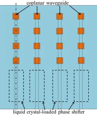
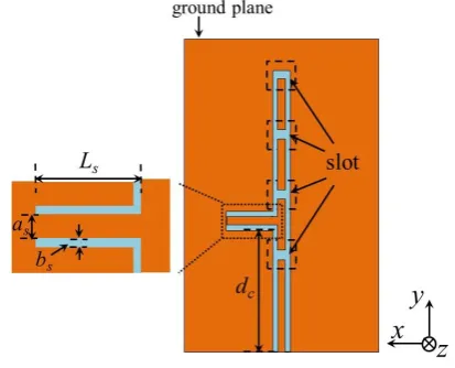
An example of the structure of a 4-element linear array antenna using open-end CPW-fed MSAs is shown in Figure 1. The radiating face is shown in (a), the feeding face is shown in (b), and a cross-section of the part at the dashed line is shown in (c). The patch width W is defined as the length of the patch in the di-rection perpendicular to the feed line, and the patch length L is defined as the length of the patch in the direction that is parallel to the feed line. The patches are arranged along a straight line, as shown in Figure 1(a). Slots are placed on the back side of the patches, as shown in Figure 1(b). The length of the slots is 100 mm, and the slots are arranged such that their centers are aligned with the centers of the patches. Considering expansion to an adaptive array antenna, we chose a linear array antenna construction for the antenna constituting the fun-damental element. Figure 2 shows a conceptual diagram of an adaptive array antenna composed of 16 elements where 4 basic elements are lined up to tilt the beam, in which the basic elements are the 4-element linear array antennas shown in Figure 1. Here, the 4-element linear array antennas are arranged in parallel, and liquid crystal-loaded phase shifters are connected to the feed lines of each one. The tilt of the maximum radiation direction of the main beam in the x-axis direction in Figure 2 can be controlled. For the design of the CPWs, the width of the central conductor is set to a = 1.80 mm, the slit width is set to b = 0.10 mm, and the distance between the centers of neighboring patches is set to the patch pitch dp so that the characteristic impedance becomes approximately 50 Ω. The printed circuit board has a dielectric thickness of h = 0.50 mm, per-mittivity of εr = 2.60, and conductor thickness of r = 0.018 mm.
2.2. Design of Linear Array Antenna Using Open-End CPW-Fed MSAs
(a) (b)
[image:4.595.212.538.72.390.2](c)
Figure 1. Structure of linear array antenna with microstrip patch antennas fed by the open end of coplanar waveguides. (a) Radiating face; (b) Feeding face; (c) Cross-section.
Figure 2. Adaptive array antenna with liquid crystal-loaded phase shifters.
element spacing has a large impact on the relative phase between the elements. The equation for the relationship between the element spacing and the maxi-mum radiation direction in the linear array antenna is shown in Equation (1)
[11].
0
sin w p
[image:4.595.293.454.431.621.2]Here, θ represents the offset at the x = 0 face where the z-axis direction is tak-en to be 0˚, and λ0 represents the free space wavelength. The maximum radiation direction is designed to be in the z-axis direction, θ = 0, so the effective wave-length on the feed line waveguide λg is obtained according to Equation (2).
0
p g
w
d λ λ
ε
= = (2)
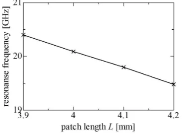
Based on Equation (2), when making the maximum radiation direction face in the z-axis direction, the element spacing should be set to be equivalent to one wavelength of the radiated electromagnetic wave. Therefore, the element spacing dp was made to vary within the range 11.00 - 13.50 mm which corresponds to 0.9 λg - 1.1 λg, and the electromagnetic field simulation software was used to calcu-late the changes in the maximum radiation direction. As a result of optimizing the size of the patch in the design of one element [10], we obtained W = 6.90 mm and L = 3.90 mm. In Figure 3, an offset of the maximum radiation direction from the z-axis to the positive y-axis direction is defined to be positive. When the element spacing dp was 11.00 mm, the offset angle became 0˚. The radiation characteristics for this situation at 20 GHz are shown in Figure 4, and the fre-quency characteristics of the reflection loss are shown in Figure 5. Figure 4
Figure 3. Variation of radiation direction by space between elements.
Figure 4. Radiation characteristics of the linear array antenna for dp = 11.00 mm.
Figure 5. Return loss S11 of the linear array antenna for dp = 11.00 mm.
[image:6.595.281.465.412.548.2] [image:6.595.281.465.583.718.2]Figure 7. Variation of return loss for patch width W.
[image:7.595.281.468.417.563.2]Figure 8. Return loss of the optimal design.
Figure 9. Radiation characteristics of the optimal design.
seen that resonance points exist at frequencies other than 20 GHz. The results in
Figure 10. Radiation characteristics for undesirable resonance frequency.
3. Structure of Stub-Loaded Linear Array Antenna
3.1. Investigation of Impedance-Matching Circuit (Stub)
The 4-element linear antenna considered in the previous section had multiple resonance points. It was demonstrated that the maximum radiation direction changes for resonance points other than 20 GHz. In this section, we discuss the results of our investigation on placing an impedance-matching circuit on the CPW as a method for solving this problem. Previous studies have reported the creation of filters using short stubs for CPWs [12]. According to reference [12], the impedance Zl of the load side separated from the transmission line of line length l can be represented by Equation (3).
0 0 0 2 tan 2 tan l g l l g
Z jZ l
Z Z
Z jZ l
π λ π λ + =
+
(3)
To match impedances, the reactance of the parallel stub is represented as jX, and the designer should connect a circuit with jX needed to cancel the imaginary part of Zl shown in Equation (3). Here, the parameters of the stub that can be adjusted include the line length l and stub reactance jX. Considering the imped-ance of the stub side as viewed from the feed line, the short stub represents the case where Zl = 0 in Equation (3), so it can be expressed as shown in Equation (4).
0 2 tan
l
g
Z jZ πl
λ
′ = (4)
In the 4-element linear array antenna considered here, it is necessary to adjust the impedance-matching circuit to suppress the resonances at frequencies other than the design frequency of 20 GHz. In other words, setting the line length l to λg/2 so that Zl in Equation (4) becomes zero changes the impedance at wave-lengths other than λg, making it is possible to suppress the undesired resonance points at frequencies other than 20 GHz.
3.2. Design of the Stub Circuit
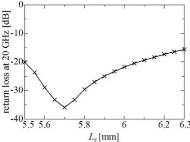
an-tenna under consideration is shown in Figure 11. A short stub with a shortened tip is used. The stub length is defined as Ls, and the distance from the feed point to the stub is defined as dc. The central conductor width and slit width of the stub are a = 1.80 mm and b = 0.10 mm, similar to the feed line. The adjustable parameters of the stub include the stub length and the stub arrangement posi-tions. In this investigation, we set the stub length Ls to λg/2 = 6.10 mm, and ana-lyzed the changes in the antenna characteristics with respect to changes in dc using the electromagnetic field simulation software. The return loss S11 at 20 GHz is shown in Figure 12. The largest return loss of −25.22 dB was obtained when dc = 37.50 mm. Next, we analyzed the changes in the characteristics with respect to changes in the stub length Ls. The changes in return loss at 20 GHz are shown in Figure 13. Because we obtained S11 = −46.5 dB when the stub length was Ls = 5.95 mm, we determined that this is the optimal value. Furthermore, the frequency characteristics of the return loss for this situation are shown in
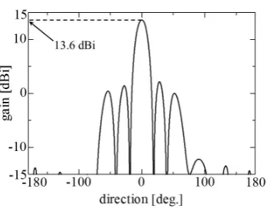
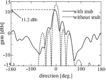
[image:9.595.284.465.584.713.2]Figure 14, and the radiation characteristics are shown in Figure 15. The solid line shows the return loss frequency characteristics for the case with the stub, and the dotted line shows the characteristics for the case without the stub. Fig-ure 14 shows that the undesired resonances are suppressed well, and that the return loss at the design frequency has been improved. On the other hand, as shown in Figure 15, the gain in the maximum radiation direction decreased.
Figure 11. Structure of the stub circuit.
Figure 13. Variation of return loss by stub length LS.
Figure 14. Return loss of the linear array antenna with stub.
Figure 15. Radiation characteristics of linear array antenna with stub.
While the gain was 13.6 dBi without the stub, the gain was 11.2 dBi with the stub. This is believed to be caused by the stub radiating waves from the face with the feed line at the back of the antenna. In addition, the side lobes increased.
3.3. Design of Stub Circuit with Slits
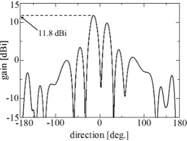
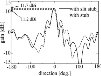
[image:10.595.283.466.416.554.2]coupling between the stubs. This is done by generating aperture coupling be-tween the stubs by creating slits within the stubs. Since the value of λg in the stub circuits may change due to the slits, we performed optimization of the stub length Ls. Figure 17 shows the changes in the return loss with respect to the stub length Ls. When Ls = 5.70 mm, S11 = −42.53 dB, and fr = 19.99 GHz. This was chosen as the optimal value. The return loss for this situation is shown in Figure 18, and the radiation characteristics are shown in Figure 19. For return loss, the
[image:11.595.278.466.404.544.2]Figure 16. Structure of stub circuit with slits.
Figure 17. Variation of return loss by stub length LS.
[image:11.595.280.467.577.716.2]Figure 19. Characteristics of te linear array antenna with slit stub.
undesired resonances were suppressed after loading with the stub as well, and no large changes were seen. For radiation characteristics, on the other hand, a gain improvement of 0.5 dBi was seen.
4. Conclusion
We investigated the design of a linear array patch antenna composed of 4-ele- ment linear array antennas using four 20 GHz band MSAs with a structure such that the signal is fed to the patch antennas from open-end CPWs without con-tact. To adjust the maximum radiation direction and reduce the return loss, we optimized the element spacing and the element shape, and obtained a return loss of −29.59 dB at the resonance frequency of 20.05 GHz. However, undesired re-sonance frequencies gave rise to frequency bands other than the design frequen-cy of 20 GHz when a 4-element linear array antenna structure was used. To suppress these undesired resonances, we proposed a new structure in which the feed line is loaded with a short stub as a method to obtain stable performance at the design frequency. We demonstrated that this method can sufficiently sup-press the undesired resonances. Furthermore, we revealed that introducing the short stub causes a new problem in which the radiation gain is reduced. To solve this problem, we proposed a design method for a new structure in which the circuit has slits between the stubs, which improved the antenna gain by 0.5 dBi.
In the future, we plan to investigate methods for further improving the max-imum radiation gain of a linear array of patch antennas that is designed using the design method proposed in this paper.
References
[1] International Telecommunication Union (2016) Use of the Frequency Bands 19.7 - 20.2 GHz and 29.5 - 30.0 GHz by Earth Stations in Motion Communicating with Geostationary Space Stations in the Fixed Satellite Service. Resolution 156. Pro-ceedings of the World Radiocommunication Conference (WRC-15), Geneva, 2-27 November 2015.
II: Electronics), 86, 49-60. https://doi.org/10.1002/ecjb.10130
[3] Utsumi, Y., Kamei, T., Saito, K. and Moritake, H. (2005) Increasing the Speed of Microstrip-Line-Type Polymer-Dispersed Liquid-Crystal Loaded Variable Phase Shifter. IEEE Transactions on Microwave Theory and Techniques, 53, 3345-3353.
https://doi.org/10.1109/TMTT.2005.857123
[4] Utsumi, Y., Kamei, T., Maeda, T. and Dinh, N.Q. (2007) Microwave High-Speed Liquid Crystal Devices Using CPW with Floating Electrode. Molecular Crystals and Liquid Crystals, 476, 249-259. https://doi.org/10.1080/15421400701739121
[5] International Telecommunication Union (2012) Recommendation, ITU-R BO. 1776-1. Maximum Power Flux-Density for the Broadcasting-Satellite Service in the Band 21.4-22.0 GHz in Regions 1 and 3. International Telecommunication Union, Geneva.
[6] Kamei, T., Yokota, M., Ozaki, R., Moritake, H. and Onodera, N. (2011) Microstrip Array Antenna with Liquid Crystals Loaded Phase Shifter. Molecular Crystals and Liquid Crystals, 542, 689-697. https://doi.org/10.1080/15421406.2011.570555
[7] Kamei, T., Utsumi, Y., Dinh, N.Q. and Thanh, N. (2007) Wide-Band Coaxial-to- Coplanar Transition. IEICE Transactions on Electronics, E90-C, 2030-2036.
https://doi.org/10.1093/ietele/e90-c.10.2030
[8] Kamei, T., Ohshima, Y. and Kawano, T. (2014) A Study for Patch Length L of Mi-crostrip Patch Antenna Excited By Coplanar Waveguide Edge Slot. Proceedings of APCOM 2014, Tokyo, 24-27 August 2014, 76-79.
[9] Ohshima, Y., Kamei, T. and Kawano, T. (2014) Design of Microstrip Patch Antenna Excited by Coplanar Waveguide Edge Slot. Proceedings of Asia-Pacific Microwave Conference 2014, Sendai, 4-7 November 2014, FR3G-39, 1396-1398.
[10] Ohshima, Y., Kamei, T. and Kawano,T. (2015) A Study for Design of Microstrip Patch Antenna Fed by Open-End of Coplanar Waveguide. IEICE Transactions on Electronics, J98-C, 348-355.
[11] Lalezari, F. and Massey, C.D. (1987) MM-Wave Microstrip Antennas. Microwave Journal, 30, 87-96.
[12] Takiguchi, Y., Ma, Z. and Kobayashi, Y. (2000) SCE2000-26/MW2000-90 Design of a Novel 30 GHz Band-Pass Filter Using Coplanar Waveguide Structures [in Japa-nese].Technical Report of IEICE,100, 105-109.
Submit or recommend next manuscript to SCIRP and we will provide best service for you:
Accepting pre-submission inquiries through Email, Facebook, LinkedIn, Twitter, etc. A wide selection of journals (inclusive of 9 subjects, more than 200 journals)
Providing 24-hour high-quality service User-friendly online submission system Fair and swift peer-review system
Efficient typesetting and proofreading procedure
Display of the result of downloads and visits, as well as the number of cited articles Maximum dissemination of your research work