Behavioural Modelling Of Single Stage
Discrete Time Sigma Delta Modulator
Anjli Shukla1, Mr. Anil Kumar Sahu2 1
M.E. Scholar, VLSI Design, Electronics & Telecommunication Department, Student of Engineering & Technology, Shri Shancharacharya Technical Campus, Bhilai, Chhattisgarh, India,
2
Assistant Professor, Electronics & Telecommunication Department, Faculty of Engineering & Technology ,Shri Shancharacharya Technical Campus, Bhilai, Chhattisgarh, India
Abstract— Modulator is one of the most significant building-blocks in integrated discrete time component used in
Sigma-Delta (ΣΔ) analog to digital converter. In this paper a novel structure of a discrete time first order modulator Sigma-Delta is
implemented at a supply voltage of 3 V. The designed modulator has a resolution of 8 bits at a sampling frequency of 10.25 MHz Eventually the modulator consume only 1.16 mW of power under 3V.
Keywords— Sigma delta modulator, Switched capacitor circuits, Analog-to-digital converter (ADC), Digital-to-analog converter (DAC), Digital filter.
I.INTRODUCTION
A. Sigma-Delta Modulation (SDM)
[image:2.612.262.412.448.503.2]As the name imply in a sigma-delta modulation (SDM) the input is integrated (sigma) prior to delta modulation coding. The signal amplitude remains constant with the increasing frequency, hence SDM is also known as pulsation density modulation (PDM). In SDM signal is been quantized directly and not its copied as in Delta Modulation (DM). Hence greatest quantizer range is determined by the maximum signal amplitude and is not dependent on the signal spectrum. The SDM is achieved by over-sampling the input data and determining the quantization noise. Switched-capacitor (SC) integrators and amplifiers are the basic building blocks of Al modulators and pipelined ADCs, respectively. One of the most challenging aspects in the behavioral simulation of an SC stage (amplifier or integrator) is the modeling of the circuit non-idealities in its opamp. Hence, this paper proposes an logical model for the behavioral simulation of the effect of opamp gain and dynamics on the gain of an SC amplifier and the transfer purpose of an SC integrator.
Fig 1: Block diagram of first order sigma delta modulator
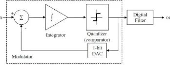
The basic block diagram of a discrete-time first order ΣΔ modulator is shown in figure 2. The input signal comes into the modulator via a summing block. It then passes through the integrator which feeds a comparator that acts as a one-bit quantizer. The comparator output is fed back to the input summing junction via a one-bit digital to analog converter (DAC), and it also passes through the digital filter and emerges at the output of the converter.
Fig 2: Discrete time first order sigma delta modulator
1) Over-Sampling: Extra dynamic range can be achieved by spreading the quantization noise power over a larger frequency range. The amplify in the dynamic range is only 3dB for every doubling of the example frequency.
[image:2.612.241.415.584.651.2]out of the band. But the in general noise remains the same for the entire band.
B. Principles Of Sigma Delta ADC
The process of sampling and quantization is standard approach for conversion of analog signals to digital. Normally sampling is performed at nyquist rate i.e. at fs=2fm and then quantization is done. The quantizer being a non linear device will introduce a quantization noise. The SQNR (Signal to Quantization Noise) of such an ADC for an N bit quantizer with a chirp signal input is modelled as follows
SQNR= 6.02N + 1.76 dB
This is commonly known as the 6-dB rule for delta modulation. In SDADC, effort is made to reduce the quantization noise by sampling the signal very closely. Sampling is done at a much higher rate than the nyquist rate (fs>>2fm) and OSR = fs/2fm. This is typically between 16-512 times the nyquist rate and hence is suitable for audio application. It improves the SQNR by a great amount as shown below.
SQNR = 6.02N + 10 Log (OSR) +1.76 dB
The presentation is improved more by doing noise shaping by introducing a loop filter wherein the quantization error is moved out to the filter stop band, thus reducing the in band noise, thus increasing the SQNR. Further, the SQNR can be increased by increasing the order of the modulator to get a sharp cut-off. The effect of noise shaping is clear from the following equation wherein L stands for the order of the filter.
SQNR=6.02N+ 10(2L+1)Log (OSR)+1.76dB
Higher order modulators will lead to instability of the circuit and hence a feedback path is introduced to keep the system stable. It is here we observe that a difference and summation (loop filter) is being perform together.
C. Delta-Sigma Modulator
A general simplified block diagram of a digital Delta-Sigma modulator is shown in figure 1. A delta sigma modulator consists of three main components: a loop filter (or loop transfer function H(z)), an analog-to-digital converter (or a clocked quantizer), and a feedback digital-to-analog converter (DAC) . As in the block diagram, the input goes through the loop filter and then is converted to a digital word sequence whose spectrum approximates the input well in a narrow frequency range but with quantization noise. In the feedback loop, the digital output is then converted back to an analog signal which is fed back into the loop filter, and then the loop filter can “shape” the quantization noise away from the preferred frequency range. This is how delta-sigma modulator workings as an analog-to-digital converter.
1) Over-Sampling: As we know, the Nyquist theorem states that in order to fully recover a sampled input signal, the samples must be taken at frequency greater than two times the bandwidth of the input signal. Aliasing will occur and the recovered signal will have deformation if the sampling frequency does not meet requirements. Oversampling means sampling at a frequency much greater than the Nyquist frequency. We define the oversampling ratio (OSR) as the sampling frequency fs over Nyquist frequency fN. Compared to the Nyquist-rate data converters, over-sampled ΔΣM have demonstrated lower sensitivity to the analog component imperfection, credit to a higher sampling rate and more complex digital signal processing. Quantization noise occur when discrete-time analog sample values are converted to finite-state numbers. Oversampling will not reduce the amount of total quantization noise, but it will spread the noise across a larger frequency spectrum so that the rule of in-band quantization noise is reduced. Delta-sigma techniques make use of this characteristic by following the converter with a decimation filter and remove the high frequency noise.
2) Noise Shaping Technique: Noise shaping is added used to reduce the noise power in the signal band. Its purpose is to increase the apparent signal-to-noise ratio (SNR) of the resulting signal by altering the spectral shape of the error that is introduced by quantization such that the noise power is at a lower level in frequency bands at which noise is perceived to be more undesirable and at a correspondingly higher level in bands where it is perceived to be less need. Noise shaping happens because of the loop filter transfer function of a ΔΣM is collected of a STF and a NTF. The STF is designed to have steady gain over all frequencies, while the NTF is designed to have small gain at lower frequencies. Therefore, the NTF can be designed to have minimum gain around the band of interest. When followed by a filter, much of the noise can be remove.
Fig 3: Block diagram of First Order Sigma-Delta Modulator using MATLAB/Simulink
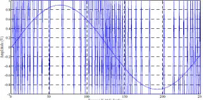
[image:4.612.236.380.260.331.2]First order ΣΔ modulators are probably the most common category of the device which has more stability than second order and third order circuit. If we compare first order ΣΔ modulator with the other types in terms of power consumption and size they consumed low power. In addition, the structure of first order ΣΔ modulator has the advantages of being simple, robust and stable. The functional diagram of the first order modulator simulated using Simulink in MATLAB is shown in figure 3. The single bit DAC is replaced by a simple wire. The input is a sinusoidal signal with 0.9 V amplitude and frequency 40 kHz. This signal is fed through only one integrator and is connected to the comparator at the output. The modulated output as seen through the scope is shown in figure 4 with the input signal overlaid on it. Behavioural simulations using MATLAB were carried out to find the optimal number of bits.
Fig 4: Delta Sigma Modulation of a Sample Waveform
[image:4.612.246.374.390.459.2]From figure 5, it can be concluded the frequency spectrum of the output that Spurious Free Dynamic Range (SFDR), which is the ratio of the RMS value of the input sine wave for an ADC to the RMS value of the peak spur observed in the frequency being 55.15 dB.
Fig 5: Output power spectrum using MATLAB/Simulink
III.DESIGNOFTHEFIRSTORDERSIGMA-DELTAMODULATOR
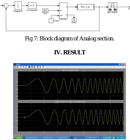
Figure 6 shows a block diagram of a complete first order ΣΔ modulator using MATLAB/SIMULINK. It is made up of an analog section, digital filter, decimation filter, look up table, a comparator, a clock generator and a voltage source of 1.5V.
Fig 6: A complete First order Sigma-Delta modulator using MATLAB/SIMULINK
A. Chirp Signal
Chirp signal is provided at the input of the analog section, output a linear chirp signal (sine wave whose frequency varies linearly with time).
B. Analog Section
[image:4.612.191.416.548.633.2]for space between ports (e.g.++|-|++) scalar, greater than or equal to, specifies the number of input ports to be summed. When there is only one input port, add /subtract elements over all dimensions or one specified dimension. The input value integrates and comparator compares the value and output passes through the input of D flip-flop. The DAC converts the Boolean input to a binary output. Rate Transition handles transfer of data between ports operating at different rates. Configuration options allow you to trade off transfer delay and code efficiency for safety and determinism of data transfer.
[image:5.612.188.408.170.406.2]Digital Filter Independently filter each channel of the input over time using a specified digital filter implementation. You can specify filter coefficients using either tunable mask dialog parameters or separate input ports, which are useful for time-varying coefficients.
Fig 7: Block diagram of Analog section.
IV. RESULT
Fig 8: The output waveform of first order fixed point sigma-delta ADC
V. CONCLUSIONS
A Sigma delta Analog to digital Convertor is designed by integrating the components of the system. It has emerged as an important technique for high resolution and high speed analog-to-digital conversion. The simple design helps in the smooth operation of the integrator circuit. This is also used as a summing circuit which helps in providing the differential feed back input to the integrator.
REFERENCES
[1] Principal for sigma delta modulation for ADC- by Sangil Park, Ph. D. Strategic Applications, Digital Signal Processor Operation.
[2] Ali Mesgarani, Khosrow H.Sadeghi, Suat U. Ay, Continuous-Time/Discrete-Time (CT/DT) Cascaded Sigma-Delta Modulator for High Resolution and Wideband Applications, 2014.
[3] Rouzbeh Jahani, Heidar Ali Shayanfar, Alireza Gharegozi, Mohsen Tamaddon, Discrete Time Sigma-Delta Modulator with the Objective of Power Consumption Reduction with 130 um Technology, in IJECCE, Vol 5, issue5, 2014.
[5] S. Pavan, N. Krishnapura, R. Pandarinathan, P. Sankar, “A Power Optimized Continuous-Time ΔΣ ADC for Audio Applications”, IEEE J. Solid-State Circuits, vol. 43, no. 2,pp. 35–360, 2008.
[6] George I Bourdopoulos, Aristodemos Pnevmatikakis, Vassilis Anastassopoulos, Theodore L Deliyannis: Delta sigma Modulators, model, Design & simulation. Imperial college press, 2006 .
[7] J. Ruiz-Amaya, J.M. de la Rosa, F. Medeiro, F.V. Fernández, R. del Río, B. Pérez-Verdú and A. Rodríguez-Vázquez, MATLAB/SIMULINK-Based High-Level Synthesis of Discrete-Time and Continuous-Time Sigma-Delta Modulators, IEEE 2004.
[8] Y. Zhu, S.F. Al-Sarawi, C. C. Lim, and M.J. Liebelt, Fourth-Order Discrete-Time Variable Centre Frequency Bandpass Sigma-Delta Modulator IEEE 2006. [9] Zhu, Y., Al-Sarawi, S. F., & Liebelt, M. J. (2006, December). Fourth-order discrete-time variable centre frequency bandpass sigma-delta modulator. In Circuits and Systems, 2006. APCCAS 2006. IEEE Asia Pacific Conference on (pp. 820-823). IEEE.
[10] T. K. Bandopadyay , Manish Saxena, Raghav Shrivastava, Sigma Delta Modulator with Improved Performance through Evolutionary Algorithm International Journal of Science and Research (IJSR) Volume 2 Issue 3, March 2013.
[11] Nagaraj, P., & Yellampalli, S. 8 Bit Second-Order Continuous-Time Band-Pass Sigma-Delta ADC. International Journal of Innovative Technology and Exploring Engineering (IJITEE),Vol.3, Issue.1,June 2013.