© 2016, IRJET | Impact Factor value: 4.45 | ISO 9001:2008 Certified Journal | Page 1400
Rohitsingh Khursel, Shubhangi Ugale, R.W.Jasutkar
PG(MTECH 4th SEM)Dept Of Electronic and Communication Engineering, G.H.Raisoni Academy of Engineering and
Technology, Maharashtra, India
Asst.Prof. Dept Of Electronics and Communication Engineering, G.H.Raisoni Academy Of Engineering and Technology, Maharashtra, India
,Asst.Prof. Dept Of Electronics and Communication Engineering, G.H.Raisoni Academy Of Engineering and Technology, Maharashtra, India
---***---Abstract –
This paper proposes low complexity and low power consumption design of 2nd order sigma-delta modulator using reversible logic gates. The proposed design constitutes modification in the integrator part of the block diagram of the 2nd order Sigma-Delta Modulator which constitutes two op-amps. The proposed design will be better in terms of low power consumption and increase in speed. The modification is done in the integrator part of op-amp. Two reversible gates has been used in the integrator part of the 2nd order sigma-delta modulator. Fredkin and toffoli gates have been used for the modification purpose. Individual blocks would be design in 0.9nm CMOS technology and are integrated. Spice based simulation is carried out on individual blocks of the circuit in the tanner tool V.13.Key Words: Sigma-Delta Modulator (ΣΔ), SC (Switched
capacitor), Fredkin gate (FG), Toffoli gate (TG), CMFBC (Common mode feedback circuit), Operational Amplifier (Op-Amp), Continuous time (CT).
1.INTRODUCTION
A 2nd order ΣΔ is a oversampled type of analog to digital convertor. Oversampling ADC has only one type that is ΣΔ modulator. Oversampling convertor is able to achieve much higher resolution than the Nyquist rate convertors. The accuracy of these convertors doesn’t depend upon the component matching, precise sample and hold circuitry or trimming and hence they reduce circuit complexity up to a greater extent. Oversampling convertors uses switched capacitors and hence does not need any dedicated sample and hold circuit. ΣΔ ADC is also called as noise shaping ADC. In ΣΔ modulator the signal is modeled at a much higher rate as compared to the Nyquist rate. A low resolution quantizer is used within the feedback configuration to model the slight noise that comes during the conversion.
ΣΔ is a robust technique of implementing high resolution analog to digital convertor in modern VLSI
technique. The main advantage of the oversampling based technique is that the higher order filtering is done in the digital domain and that it doesn’t impose any stringent requirements on the analog blocks of the modulator. There are other higher order models available ΣΔ which are being used for higher resolution though they are highly unstable, but the 2nd order gives
enough margins and can operate at a comparatively lower sampling frequency and is more stable as compared to the other orders of SDM. In this our aim is to modify the basic structure of 2nd order SDM.
Second order Sigma-Delta modulator using reversible gates and reduce the overall power consumption of the circuit.
1.1 Second Order Sigma-Delta Modulator
Above Fig1.1 shows the block diagram of 2nd order
Sigma-Delta modulator. In this block diagram there are two switched capacitor based integrator and 1bit quantizer circuit which is nothing but a comparator. In this the analog signal is being sampled at a sampling frequency of fs, the quantizer used here is one bit which has only two values +-Δ/2 which can be modeled as a quantizer error e(n) to its input which is the so called difference between the output and the input i.e +-Δ/2 , then we can treat the quantizer error as white noise E(Z). The transfer function of the 2nd order sigma-delta
modulator is given by
© 2016, IRJET | Impact Factor value: 4.45 | ISO 9001:2008 Certified Journal | Page 1401
Fig1.1 Block diagram of 2nd order sigma-Delta Modulator
For the design and integration of a second order sigma-delta modulator it is important to gauge the sensitivity of the system’s performance to various circuit non-idealities. There are several non-idealities that are characteristics for analog circuit implementation.
1.2 Switched Capacitor Based Intgrator
Fig1.2 shows fully differential switched capacitor integrator used in the 2nd order sigma-delta modulator
circuit. As the sigma-delta modulators are sampled data system, they are readily implemented using switched capacitor (SC) circuit in CMOS technology. The reason for adopting the differential configuration is that to ensure power supply rejection, clock feed through, lower switch charge injection errors and increased dynamic range.
Fig1.2.1 Switched Capacitor Implementation of 2nd order modulator
The switched capacitor based integrator with a differential architecture is shown in fig1.2.1. This particular structure ensures accuracy of the transfer function across variation and improves the dynamic range of the modulator by two-fold.
2. Reversible Logic Gates
Reversible logic has gained great attention in recent years because of their ability to reduce power dissipation which forms the main requirement in low power VLSI design. It has many area of applications in low power CMOS and optical information processing, DNA computing quantum computation and nanotechnology. According to launder’s the amount of energy dissipated for every irreversible bit operation is at least KTlN2 joules, K is the Boltzmann constant and T is the temperature at which operation is performed. A reversible logic gate is an n-input an n-output logic device with one to one mapping. This helps to determine the output from the input and also the inputs can be uniquely recovered from the outputs. In reversible logic fan-out is not possible as one-to-many concept is not reversible. The important reversible gates used for reversible logic synthesis are feyman gate, fredkin gate, toffoli gate, peres gate, and new gate sayem gate etc.
In our design of 2nd order sigma-delta modulator we
are modifying the switched capacitor based integrator and bit quantizer circuit. For the same we are using fredkin gate and toffoli gate get desired modification.
2.1. Fredkin Gate
Fredkin gate is 3*3 input and output gate. The input vector is I (A,B,C) and the output vector is O (P,Q,R). The quantum cost of a fredkin gate is 5.
Fig 2.1 Fredkin Gate
The proposed transistor implementation of the fredkin gate which requires only 4 transistor, hence the area is very low . The transistor implementation along with the waveforms obtained is shown in figure 2.1 and 2.1.1
© 2016, IRJET | Impact Factor value: 4.45 | ISO 9001:2008 Certified Journal | Page 1402 IEEE, SI, MKS, CGS, sc, dc, and rms do not have to be defined.
Fig 2.1.1 Transistor Implementation of Fredkin Gate
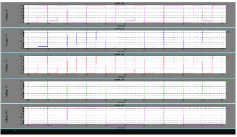
Fredkin gate is able perform backward and forward computation because of its nature. The above figure shows the waveform of the fredkin gate obtained by the simulation of the transistor implementation of the fredkin gate. The waveforms shows that the fredkin gate operates at a very low voltage and can be used in a circuit to overcame the power of any circuit.
2.2 Toffoli Gate
Toffoli gate is a 3*3 reversible gate. The input vector I (A,B,C) and output vector is O (P,Q,R). Quantum cost of a toffoli gate is 5.
The proposed Transistor implementation of toffoli gate uses 12 transistors. In the implementation the
outputs P and Q are directly generated from inputs A and B by hardwiring. This gate also performs the
forward and backward computation as our fredkin gate does.
Fig 2.2 Transistor Implementation of toffoli gate
toffoli gate and the obtained waveform.
Fig 2.2.1 Transistor Implementation of Fredkin Gate
Again the waveform shows that the reversible toffoli gate can be operated at a low voltage and can be used in other circuit to reduce the power consumption of that circuit.
[image:3.595.38.277.337.475.2]The two reversible gates we have discussed are being used in the circuit for our desired modification. Above table shows a comparison between reversible gates we are using and other types as shown in fig.2.2.1 as given below.
Fig.2.2.1 Comparison between reversible gates
Reversible gates
Quantum cost
Types No of
transistors
No of Gates
Cnot 1 2*2 5 1
Feynman 1 2*2 8 1
Fredkin 5 3*3 4 7
Toffoli 5 3*3 12 2
© 2016, IRJET | Impact Factor value: 4.45 | ISO 9001:2008 Certified Journal | Page 1403 3. Proposed Op-Amp Circuit
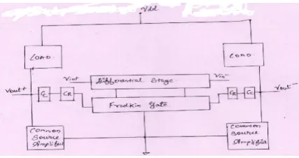
The circuit we are using for op-amp is a switched capacitor based integrator as shown in figure.3. The proposed amplifier structure shown in which NMOS cascade current source has split into two equal-sized, cross-coupled devices(M51, M52, M61, M62) with their gates connected to the outputs of the first stage (nodes n3 and nodes n4). Because of the differential structure, the common mode output voltage of both stages needs to be regulated using CMFB circuit.
The cross-coupled form the negative feedback connections which causes the differential signal at the output of the first stage to have high load impedance which is given by the equation (2) given below
gdsout1 = gds8 + (gm51 � gm52)+ gds3(gds1 + 2gds51)
gds3+gds1+2gds51+gm3+gmb3 (2)
Fig.3. Proposed Op-Amp Schematic
In the first stage the NMOS cross-coupled arrangement forms the CMFB circuit which is in-built due to these we don’t have to attach CMFB circuit for common mode input to be regulated.
The second stage consists of NMOS common source amplifier M11 (M10) with active load M10(M12). Due to the absence of NMOS arrangement we need here additional CMFB circuit.
Fig 3.A. Block diagram of Switched Capacitor Integrator
[image:4.595.37.291.358.505.2]The differential signal is applied at the differential stage then the difference between the two signals is applied to the CMFB circuit which is used to regulate the signal at both the stages. Since the CMFB circuit increases the power consumption of the circuit, the design is being modified with the reversible gate as shown in figure3.1.
Fig 3.B. Block diagram of switched capacitor integrator with reversible logic gate
4. 1Bit Quantizer
[image:4.595.309.523.367.480.2]© 2016, IRJET | Impact Factor value: 4.45 | ISO 9001:2008 Certified Journal | Page 1404
Fig.4. 1Bit Quantizer
The comparator is suitable for many high speed and low power applications. Its operation clocks as it is a sequential circuit. When there is reset mode the nodes A and B are pulled up to VDD, and when clock goes high the comparator goes in the regenerative mode and M3-M4 and M5-M6 forms a positive feedback loop. As a result the difference in the current drive of M1–M2, the voltage values at node A and B are amplified to full-scale rail to rail output. After the comparator has made the decision, the regenerative cross-coupled transistor immediately close the connections from Vdd to Gnd, this result in less power consumption.
The main objective of the project is to minimize the power consumption of the 2nd order Sigma-Delta
modulator as shown in fig.4.
5. Implemented Design Of Normal Op-Amp
The Implemented design of normal Switched capacitor integrator without the use of reversible logic gates. Here the op-amp performs the normal operation of amplification since the reversible gates are not used it. So the total power consumption of this op-amp will be high.
Fig 5. Implemented Design of Normal Op-amp
5.1 Implemented Design of Op-Amp with reversible gates
© 2016, IRJET | Impact Factor value: 4.45 | ISO 9001:2008 Certified Journal | Page 1405
The above figure shows is the modified op-amp with reversible gates. By doing this the power consumption of the circuit is reduced to greater extent as compared to normal Op-Amp circuit.
5.3 Implemented Design of 2nd Order SDM with
Reversible Gates
Fig. 5.3 Implemented Design of 2nd Order SDM with Reversible gates
The above is the implemented diagram of 2nd order
SDM with reversible gates. Thus by doing this modification the entire circuit power consumption has been reduced as compared to the previous circuit of 2nd
order SDM without reversible gates.
6. CONCLUSION
6.1 Output Of normal Op-Amp
The output shows that the op-amp performs the normal operation of amplification of the difference between the two signals.
Fig.6.1 Output of Normal Op-Amp
6.2 Output of Op-Amp With Reversible Gates
Fig.6.2 Output of Op-Amp With reversible Gates
© 2016, IRJET | Impact Factor value: 4.45 | ISO 9001:2008 Certified Journal | Page 1406 Gates
Fig.6.3 Output of 2nd Order SDM with reversible gates
From the above paper we can conclude that for 2nd
order Sigma-Delta modulator, a low voltage fully differential switched capacitor integrator is used and it also consumes less power. Reversible gates due to their reversibility can be used for further power consumption reduction in 2nd order sigma-delta
modulator. We have used 0.90nm CMOS technology for the simulation of the two proposed reversible logic gates and presented the result in terms of waveforms. The entire deign is being implemented in tanner V13., with the entire circuit power consumption has minimized and the life period of the circuit increases.
6. REFERENCES
[1] R.Ganesh Raj, A.Karmakar, S.C.Bose, “Analysis and
design of 2nd order sigma-delta modulator for audio applications”, IEEE tran.Inf.theory, vol.8,no.10,pp.828-832,oct.2014.
[2] Prashant.R.Yelekar, Sujata.S.Chiwande, “Introduction to
reversible logic gates and its applications”, IEEE transaction on circuits and system-I.vol.61, no.7 and july 2011
[3] Hakam Bennie abd juha Kostamvaara, “Layout
prefernces concerning matching in a fully differential sigma-delta modulator design”, IEEE international
circ.Sig.process,vol.51,no2.129-130,2007.
[4] Introduction to reversible logic and its application”,
Prof. Sujata.S.Chiwande, Prof. Prashant.R.Yelekar YCCE nagpur-2nd national conferences on information technology (NCICT) 2011.
[5] Low voltage fully differential CMOS switched-capacitor
amplifiers-Traf-Sum Lee-National Yunlin university of science and technology (R.O.C).
[6] Very low voltage differential amplifier for switched
capacitor applications-M.Dessouky, A.kaiser
UPMC55/65-LIP6-ASIM, iemn-ISEN-UMR
CRS9929,France.
[7] J.Candy and G.Ctemes, “Oversampling method for A/D
and D/A conversion”, pp.I-29,IEEE press, 1992
[8] Kanhu Charan Behra , M.Santosh and B.C.Bose, “Design
of a 10bit, 5M/mS pipelined ADC for CMOS Image Sensor”, VLSI design and test Symp, Chandigarh, VDAT, 2010.
[9] Wern Ming Koe and Jing Zhang, “Undestanding the effect
of circuit non-idealities on sigms-delta modulator”, pp.94-101, oct2002.
[10] J.ERice. “A new look at reversible memory elements”,
Proceedings international syposuim on circuits and systems (ISCAS) 2006, Kos, Greece, May 21-24 2006, pp.243-246.
[11] R.Launder, “Irreversibility and heat generation in the
computational process” ,IBM journal of research and development,vil.3,pp.183-191,1961.
[12] Rangaraju H.G, Venugopal U, Muralidhara K.N, Raja K.B
,“Low power reversible parallel binary
Adder/Substractor”, International journal pf VLSI design and communication system (VLSICS) vol,no.3, sept 2010.
[13] V.Rajmohan, V.Rangnathan, “Design of counter using
reversible logic”, 978-1-4224-8679-3/11/23.00, 2011.
[14] Adaptive Sigma-Delta modulator with one-bit