University of South Carolina
Scholar Commons
Theses and Dissertations
1-1-2013
Optimal Design and Control of DC-DC Resonant
Converters For Wireless Power Transfer
Applications
Isaac Nam
University of South Carolina - Columbia
Follow this and additional works at:https://scholarcommons.sc.edu/etd
Part of theElectrical and Computer Engineering Commons
This Open Access Dissertation is brought to you by Scholar Commons. It has been accepted for inclusion in Theses and Dissertations by an authorized administrator of Scholar Commons. For more information, please [email protected].
Recommended Citation
O
PTIMALD
ESIGN ANDC
ONTROL OFDC-DC
R
ESONANTC
ONVERTERS FORW
IRELESSP
OWERT
RANSFERA
PPLICATIONSby
Isaac IL W. Nam
Bachelor of Science
University of South Carolina, 2009
Master of Science
University of South Carolina, 2011
Submitted in Partial Fulfillment of the Requirements
For the Degree of Doctor of Philosophy in
Electrical Engineering
College of Engineering and Computing
University of South Carolina
2013
Accepted by:
Enrico Santi, Major Professor
Roger Dougal, Committee Member
Mohammod Ali, Committee Member
Branko Popov, Committee Member
D
EDICATIONI dedicate this work to my father, the greatest and most loving father in the world who
A
CKNOWLEDGEMENTSI appreciate the encouragement and guidance that my advisor Dr. Enrico Santi has
given me during my research. Dr. Enrico Santi has earned enormous respect through the
depth of his knowledge and sincere care for his graduate students, and this fact has served
as an inspiration for me to become a better electrical engineer.
Also, I wish to express my gratitude to other committee members, Dr. Roger Dougal,
Dr. Mohammod Ali, and Dr. Branko Popov for encouraging me and for being an
important part in my pursuit of Ph. D.
I would like to show my appreciation to my fellow graduate students in Dr. Enrico
Santi‟s group for that we have shared useful and important knowledge through friendly
interactions.
Finally, I thank the Office of Naval Research (ONR) for the partial financial support
A
BSTRACTWireless power transfer (WPT) technology provides galvanic isolation for improved
safety and also provides reliability by eliminating the need for dedicated
connectors/adapters that can get damaged due to frequent usage. For these reasons, it has
become popular in medical implant charging and electric vehicle (EV) charging. Beyond
these niche applications, due to aesthetic features and convenience provided by the
cord-free environment, it is rapidly becoming an attractive charging solution for various
portable electronics as well as household appliances.
However, currently available WPT technology demonstrates several shortcomings and
various challenges due to allowed receiver position variation with respect to transmitter
position. For consumers, major shortcomings and challenges include lower power
transmission efficiency compared to hard-connected charging method and limited
receiver positioning flexibility. For the industry, major shortcomings and challenges
include increased cost of implementation and increased complexity in design and
control.
In order to promote adoption of WPT technology, it is important to provide good
power transmission efficiency and to improve receiver positioning flexibility while
reducing complexity in design and control of resonant converters. Also, it is important to
minimize the component count to reduce the cost of implementation.
In this research, novel optimal design methods have been developed for resonant
tank and series-parallel (SP) resonant tank. Also, a novel control method for SS resonant
converter employing a symmetrical inductive coupler has been developed. These methods
reduce complexity in analysis, design, and control. Using these methods, receiver
positioning flexibility can be improved without a large component count while minimizing
design complexity. Various simulation results and experimental results are presented to
show that these methods allow achieving an optimal compromise between power
transmission efficiency and power delivery robustness against variations in resonant tank
T
ABLE OFC
ONTENTSDEDICATION ... iii
ACKNOWLEDGEMENTS ... iv
ABSTRACT ... v
LIST OF TABLES ... x
LIST OF FIGURES ... xii
LIST OF SYMBOLS ... xix
LIST OF ABBREVIATIONS ...xx
CHAPTER 1INTRODUCTION ... 1
1.1BASIC OVERVIEW OF WIRELESS POWER TRANSFER ... 1
1.2MOTIVATION AND RESEARCH OBJECTIVES ... 6
1.3RESEARCH SIGNIFICANCE ... 10
1.4BACKGROUND ON RESONANT CONVERTERS... 12
1.5THEORY OF OPERATION OF SSRESONANT CONVERTER OF SRTTYPE ... 28
1.6OUTLINE ... 32
CHAPTER 2SUMMARY DESCRIPTION OF EXPERIMENTAL EVALUATION BOARD ... 35
2.1DESCRIPTION OF EVALUATION BOARD ... 35
2.2EVALUATION OF EXPERIMENTAL SET-UP ... 41
CHAPTER 3OPTIMAL DESIGN METHOD FOR SSRESONANT TANK OF SRTTYPE TO ALLOW RAPID AND CONVENIENT CALCULATION OF PARAMETERS ... 47
3.1INTRODUCTION ... 47
3.3FREQUENCY-DOMAIN CHARACTERISTICS
OF SSRESONANT TANK OF SRTTYPE ... 52
3.4NOVEL OPTIMAL DESIGN METHOD FOR THE SSRESONANT TANK OF SRTTYPE ... 65
3.5EVALUATION AND VALIDATION OF THE PRESENTED DESIGN EQUATIONS ... 76
3.6CHAPTER SUMMARY... 84
CHAPTER 4NOVEL UNITY GAIN FREQUENCY TRACKING (UGFT)CONTROL OF SERIES -SERIES (SS)RESONANT CONVERTER OF SRTTYPE TO IMPROVE EFFICIENCY AND RECEIVER POSITIONING FLEXIBILITY IN WIRELESS CHARGING OF PORTABLE ELECTRONICS ... 86
4.1INTRODUCTION AND LITERATURE REVIEW ... 86
4.2CHARACTERISTICS OF SERIES-SERIES (SS)RESONANT CONVERTER ... 88
4.3NOVEL UNITY GAIN FREQUENCY TRACKING (UGFT)CONTROL METHOD ... 99
4.4VALIDATION ... 105
4.5CHAPTER SUMMARY... 118
CHAPTER 5NOVEL OPTIMAL DESIGN METHODS FOR ASYMMETRICAL SERIES-SERIES RESONANT TANK AND ASYMMETRICAL SERIES-PARALLEL RESONANT TANK IN LOOSELY-COUPLED WIRELESS POWER TRANSFER APPLICATIONS ... 120
5.1INTRODUCTION AND LITERATURE REVIEW ... 120
5.2DERIVATION OF GENERAL ANALYTICAL EQUATIONS IN FREQUENCY DOMAIN FOR SSRESONANT TANK TOPOLOGY ... 126
5.3DERIVATION OF GENERAL ANALYTICAL EQUATIONS IN FREQUENCY DOMAIN FOR SPRESONANT TANK TOPOLOGY ... 136
5.4SUMMARY OF GENERAL ANALYTICAL EQUATIONS AND DESIGN EQUATIONS . 148 5.5ANALYTICAL COMPARATIVE STUDY ON SS AND SPRESONANT TANK TOPOLOGIES ... 149
5.6HOW TO DESIGN RESONANT TANK TO EXHIBIT OPTIMAL QL ... 169
5.7EXPERIMENTAL RESULTS OF OPTIMAL DESIGNS ... 170
5.9CHAPTER SUMMARY... 186
CHAPTER 6CONCLUSION,PUBLICATIONS, AND FUTURE WORK ... 188
6.1CONCLUSION ... 188
6.2PUBLICATIONS ... 192
6.3FUTURE WORK ... 193
L
IST OFT
ABLESTABLE 2.1MAXIMUM OR TYPICAL RATINGS OF TRENCH GATE SILICONE MOSFET FROM
VISHAY ... 39
TABLE 2.2RATINGS OF HALF-BRIDGE DRIVER,MAX15019A(TTL), FROM MAXIM ... 40
TABLE 2.3BRIEF SPECIFICATIONS OF F28335CONTROL CARD FROM TEXAS INSTRUMENTS ... 41
TABLE 3.1EQUATIONS FOR FREQUENCIES OF INTEREST ... 56
TABLE 3.2SUMMARY OF RESONANT FREQUENCIES ... 62
TABLE 3.3DESIRED LCLCRESONANT TANK CHARACTERISTICS ... 76
TABLE 3.4EVALUATION OF THE PROPOSED PEAK VOLTAGE GAIN EQUATION ... 80
TABLE 3.5THE SSTOPOLOGY PARAMETERS CALCULATED FOR VARIOUS K'S TO ACHIEVE DESIRED ||GV||MAX USING THE PROPOSED DESIGN METHOD ... 81
TABLE 3.6EXPERIMENTAL PARAMETERS VS.PARAMETERS CALCULATED USING THE PROPOSED DESIGN METHOD ... 83
TABLE 4.1LI-ION BATTERY MODEL PARAMETERS USED IN SIMULATION ... 96
TABLE 4.2SS RESONANT TANK PARAMETERS USED IN SIMULATION ... 96
TABLE 4.3EXPERIMENTAL SSRESONANT TANK PARAMETERS ... 115
TABLE 4.4ACCURACY EVALUATION OF UGFTCONTROL MODEL EQUATION ... 116
TABLE 4.5EXPERIMENTAL EFFICIENCY DATA ... 118
TABLE 5.1EXPECTED PARAMETERS USED FOR EVALUATING QLEFFECTS FOR LS1=LS2‟ 156 TABLE 5.2PARAMETRIC SIMULATION DATA FOR EVALUATING ФVID(JΩS_SS_KMAX)SS UNDER KVARIATION WITH AN OPTIMAL QLSSACHIEVED AT K = KMAX ... 167
Table 5.4 NOMINAL PARAMETERS OF EXPERIMENTALLY-IMPLEMENTED SSRESONANT TANK... 172
TABLE 5.5EXPERIMENTAL DATA FOR ||GV(jωS_SS_kmax)||SS(λ)AND||GI(jωS_SS_kmax)||SS(ξ)
AT THREE DIFFERENT VALUES OF QLSS UNDER kVARIATION ... 173
TABLE 5.6EXPERIMENTALLY-IMPLEMENTED SPRESONANT TANK PARAMETERS ... 176
TABLE 5.7 EXPERIMENTAL DATA FOR ||GV(jωS_SP_kmax)||SP (α)
AND ||Gi(jωS_SP_kmax)||SP (β) ... 177
TABLE 5.8EXPERIMENTAL DATA FOR EVALUATING THE CIRCULATING CURRENT IN THE COUPLER ... 180
TABLE 5.9EXPERIMENTALLY-EXTRACTED T-EQUIVALENT MODEL PARAMETERS OF
ASYMMETRICAL COUPLER IN FIGURE 5.20 ... 181
TABLE 5.10SIMULATION DATA FOR ||GV(jɷs_SP_kmax)||SPFOR DIFFERENT QLSP
L
IST OFF
IGURESFigure 1.1: A magnetic coupler example consisting of two flat planar cores with 1:1 turns ratio ... 1
Figure 1.2: Simplified overview of resonant converter operation. ... 3
Figure 1.3: Series-series (SS) and series-parallel (SP) resonant tanks with secondary-side parameters referred to primary side. ... 4
Figure 1.4: DC-DC series LC resonant converter. ... 13
Figure 1.5: Square wave resonant tank input voltage, vS(t), and its fundamental frequency
component, vS(t). ... 16
Figure 1.6: Source current, ig(t), and resonant tank input current, is(t). ... 16
Figure 1.7: Diode bridge rectifier with low pass filter and load resistor. ... 17
Figure 1.8: Waveforms of the series LC resonant tank‟s output voltage vr(t), its
fundamental component vr1(t), and resonant tank output current ir(t). ... 17
Figure 1.9: Steady-state equivalent model of series LC resonant converter. ... 18
Figure 1.10: ZVS during turn-on transitions of MOSFETs in series LC resonant converter of Figure 1.4 in above-resonance operation. ... 20
Figure 1.11: MOSFET Q1 voltage and current of series LC resonant converter in above-resonance operation for ZVS. ... 21
Figure 1.12: Introduction of commutation interval, X, where charging and discharging of parallel capacitors of transistors occur for soft transistor voltage transitions. ... 21
Figure 1.13: ZCS during turn-on transitions of MOSFETs in series LC resonant converter of Figure 1.4 in above-resonance operation. ... 22
Figure 1.14: MOSFET Q1 voltage and current of series LC resonant converter in below-resonance operation for ZCS. ... 23
Figure 1.16: PWM technique for controlling resonant tank output power via active on-time variation of the switches in the secondary-side full-bridge rectifier. .... 26
Figure 1.17: Phase-shift control to apply inductive effective load. ... 27
Figure 1.18: Phase-shift control to apply capacitive effective load. ... 28
Figure 1.19: DC-DC bidirectional full-bridge SS resonant converter of SRT type... 29
Figure 1.20: The full-bridge SS resonant converter's waveforms at unity voltage gain frequency. ... 31
Figure 1.21: Simplified equivalent model of the SS resonant converter in Figure 1.19 at
fS = fO. ... 32
Figure 1.22: Equivalent circuits of the SS resonant converter for six different intervals (ta
through tg indicated in Figure 1.20) in one switching cycle. ... 32
Figure 2.1: Evaluation board implementing a SS resonant tank of SRT type containing the symmetrical pot core coupler as an example. ... 36
Figure 2.2: Power stage component diagrams DC-DC SS and SP resonant converters. .. 36
Figure 2.3: Half-bridge LCLC resonant converter's primary-side waveforms. ... 38
Figure 2.4: Full-bridge LCLC resonant converter's primary-side waveforms. ... 38
Figure 2.5: Equivalent mode of Figure 19 with the measured voltages and currents indicated. ... 42
Figure 2.6: Simulation (left) and experimental (right) results for resonant tank input voltage [VH1(t)], primary (tank input) current [iLe1(t)], output voltage [VH2(t)], and secondary current [iLe2(t)] for fS ≈ 250kHz. ... 43
Figure 2.7: Simulation (left) and experimental (right) waveforms of primary current (top), magnetizing inductance current (middle), and secondary current (bottom) for
fS ≈ 250kHz. ... 43
Figure 2.8: Simulation (left) and experimental (right) results for resonant tank input voltage [VH1(t)], primary (tank input) current [iLe1(t)], output voltage [VH2(t)], and secondary current [iLe2(t)] for Re' ≈ 8.1 Ω. ... 44
Figure 2.9: Simulation (left) and experimental (right) waveforms of primary (tank input) current [iLe1(t)], circulating current through Lm [iLm(t)], and secondary
current [iLe2(t)] for Re' ≈ 8.1 Ω. ... 44
Figure 2.11: Experimental efficiency data plot for the SS resonant converter with active
synchronous rectification (ZCS) under varied load condition. ... 46
Figure 3.1: Portions of peak voltage gain curves, used (a) in reference [20] and (b) in reference [21], showing relationship among (or coupling coefficient, k), Q, and peak voltage gain values in ZVS range (above peak resonance range). ... 50
Figure 3.2: Equivalent model for SS resonant tank of SRT type... 53
Figure 3.3: ||GV(jω)|| of SS resonant tank of SRT type for varied Re'(Q). ... 54
Figure 3.4: Normalization of resonant frequency sets. ... 56
Figure 3.5: Circulating current gain magnitude ||GiLm(jω)|| (top) and voltage gain magnitude ||GV'(jω)|| (bottom) of the SS resonant tank of SRT type. ... 58
Figure 3.6: Equivalent circuit transformation for graphical derivation of equation for fn. 59 Figure 3.7: Effects of selecting a larger value for fO in a design process. ... 59
Figure 3.8:Parametric simulation results for ||GV'(jω)|| for varied Re'. ... 60
Figure 3.9: Approximated equivalent model of SS topology when Re' (thus, Q) is high enough for ||GV||max to be well above unity. ... 61
Figure 3.10: ||GV(jω)|| of the SP topology for varied ratio of C2' to C1... 62
Figure 3.11: ||GV'(jω)|| of the SS topology when C2' = 10*C1. ... 62
Figure 3.12: Voltage gain ||GV(jω)|| curves for varied Re' showing also the frequency-dependent trends of output current level (power delivery) and efficiency. ... 65
Figure 3.13: Voltage gain of SS resonant tank at various k, when the single resonant peak behavior is achieved (a) and is not achieved (b). ... 65
Figure 3.14: FES simulation and experimental characterization of a flat spiral inductor on a ferrite disk core. ... 69
Figure 3.15: Two selected geometries for a coupler: ferrite pot core (left) and disk core (right). ... 70
Figure 3.16: Two possible symmetrical coupler geometries, Geo A and Geo B... 70
Figure 3.17: FES simulation of Geo A to extract its T-equivalent model parameters and k. ... 71
Figure 3.19: Voltage gain, ||GV(jω)||, and circulating current gain, ||GiLm(jω)||, for SS
resonant tank of SRT type employing Geo A (top two plots) and Geo B (bottom two plots). ... 74
Figure 3.20: Simulated voltage gain plot of the SS resonant tank of SRT type whose parameters are calculated by the proposed step-by-step design procedure. .. 78
Figure 3.21: Coil-to-coil distance of pot core coupler. ... 80
Figure 3.22: Comparison between ||GV||max calculated using Equation 32 and ||GV||max
determined using parametric simulations. ... 80
Figure 3.23: % error between desired ||GV||max and |||GV||max achieved using the proposed
design method for various combinations of k and desired ||GV||max (Q). ... 82
Figure 3.24: ||GV(jω)|| in dB of SS resonant tank of SRT type using Agilent 4395A
Network Analyzer. ... 83
Figure 4.1: Series-series (SS) resonant converter topology for UGFT control method. .. 88
Figure 4.2: Simplified model of the SS resonant converter in Figure 58 (a) and its
equivalent model when fS ≈ fO (b). ... 89
Figure 4.3: Effects of Q selection on voltage gain control model derivation. ... 91
Figure 4.4: Simulation results (a) and experimental results (b) of Li-ion battery
characteristics. ... 92
Figure 4.5: Efficiency, load current, and voltage gain (V2/V1) data collected at various Switching frequencies (fS) with SoC = 50% for Case A (a and b) and
Case B (c and d). ... 97
Figure 4.6: Simulink simulation data for efficiency and voltage gain (a),
and load current (b) collected at various switching frequency (fS) with SoC = 50% for Case C. ... 97
Figure 4.7: Various resonant tank waveforms and input and output currents at different SoC. (Note: Red line in the model represents the impedance compensation occurring at fs ≈ fo). ... 98
Figure 4.8: Proposed receiver topology. ... 101
Figure 4.9: Proposed operation process employing UGFT. ... 101
Figure 4.10: Voltage gain magnitude,||GV(jω)||, and phase shift, Фvid(jω), between input
Figure 4.11: Simulink model of SS resonant converter of SRT type implementing
proposed UGFT control method. ... 108
Figure 4.12: Inside of the UGFT Control block. ... 109
Figure 4.13: Inside of Fourier transformation block. ... 110
Figure 4.14: Unity-gain frequency tracking operation. ... 110
Figure 4.15: Unity-gain frequency tracking performance. ... 111
Figure 4.16: PLL operation and commutative gate signals. ... 111
Figure 4.17: Experimental setup for the SS resonant converter. ... 115
Figure 4.18: Voltage gain [||GV(jω)||] and phase shift [Фvid(jω)] (a) plotted in simulation using experimentally-extracted parameters for various k, and the linear relationship between them at fS ≈ fα (b)-Note:Rsense of 1Ω added. ... 115
Figure 4.19: SS resonant tank's input voltage, V1(t), input current, iLe1(t), and output of ultra-fast comparator whose pulse width is the phase shift, Фvid, between V1(t) and iLe1(t). ... 116
Figure 4.20: Various waveforms captured to show the UGFT control operation at k ≈ 0.83 (a) and k ≈ 0.74 (b) while performing passive diode rectification. ... 117
Figure 4.21: Various waveforms captured while operating at fO* calculated by the UGFT control model for k ≈ 0.83(a), k ≈ 0.74(b), and k ≈ 0.68(c) - Note: The output voltage (Vo) is approximately 5V while the supply voltage (Vg) of 10V is applied, indicating the operation of the SS resonant converter at fS ≈ fO*. .. 117
Figure 5.1: Voltage gain (||GV(jω)||SS), current gain (||Gi(jω)||SS), and circulating current (||GiLm(jω)||SS) for varied effective resistive load under LS1 > LS2 (a) and LS1 < LS2 (b). ... 128
Figure 5.2: Voltage gain, ||GV(jω)||SP, and current gain, ||Gi(jω)||SP, of SP resonant tank with fixed k under Re' (QLsp) variation. ... 138
Figure 5.3: Simplified transformer model of SP resonant tank ... 140
Figure 5.4: Graphical representation of input impedance, ||Zi(jω)||SP, characteristics for ||GV||max =|GV|indSP(a) and for ||GV||max >> |GV|indSP (b). ... 141
Figure 5.6: Normalized voltage gain ||GV(jω)||SPn (red curve) and normalized current gain
||Gi(jω)||SPn (green curve) plotted for the condition of QLsp = QTHsp in linear
frequency scale. ... 154
Figure 5.7: Screenshot of Ansys Maxwell 3D FES used for aiding experimental design of asymmetrical coupler (Txin circular flat-planar core and Rx in circular pot core). ... 156
Figure 5.8: SS resonant tank's voltage gain (a), current gain (b), and circulating current gain (c) with ωS_SS_kmax fixed at ωOVp_kmax = ωOVs_kmax = ωOV2_kmax for
LS1 ≈ LS2'. ... 158
Figure 5.9: SP resonant tank's voltage gain (a) and circulating current gain (b) with ωS_SP_kmax fixed at ωOV_kmax = ωOi_kmax for LS1 = LS2'. ... 159
Figure 5.10: Matlab 3D plot for ratio, GRatio, of ||GV(jωS_SS_kmax)||SS to
||Gi(jωS_SS_kmax)||SS. ... 163
Figure 5.11: Voltage gain (||GV(jω)||SS), current gain (||Gi(jω)||SS), and circulating current
gain (||GiLm(jω)||SS) under k variation for optimal QLss (left figure inside the
red box) and for 0.463*optimal QLss (right figure inside the black box - Note:
ωS_SS_kmax = 200 kHz. ... 164
Figure 5.12: Simulation plots for Фvid(jω)SS, ||GV(jω)||SS, and ||Gi(jω)||SS obtained using
the T-equivalent model parameters extracted from FES – Note:
ωS_SS_kmax=2π(300kHz). ... 167
Figure 5.13: Simulation plots for Фvid(jω)SP, ||GV(jω)||SP, and ||Gi(jω)||SP obtained using
the T-equivalent model parameters extracted from FES – Note:
ωS_SP_kmax=2π(300kHz). ... 168
Figure 5.14: Experimental setup of resonant converter evaluation board
containing experimental construction of the asymmetrical coupler shown in Figure 5.7... 171
Figure 5.15: Experimental plots for voltage gain magnitude, ||GV(jω)||SS, (a) and current
gain magnitude, ||Gi(jω)||SS, (b) of SS resonant tank. ... 173
Figure 5.16: Experimental data for GRatio (the ratio of experimental voltage gain, λ, to
experimental current gain, ξ) at LQ, Opt Q, and HQ. ... 174
Figure 5.17: Experimental plots for voltage gain magnitude, ||GV(jω)||SP, (a) and current
gain magnitude, ||Gi(jω)||SP, (b) of SP resonant tank. ... 176
Figure 5.18: Voltage gain ||GV(jωS_SP_kmax)||SP (a) and current gain ||Gi(jωS_SP_kmax)||SP
Figure 5.19: Experimental waveforms of resonant tank input voltage (V1(t) in yellow),
primary-side coil current (iLe1(t) in purple), secondary-side coil current (iLe2(t)
in green), and circulating current in the coupler (iLe1(t)- iLe2(t) in red) for LQ:
QLsp ≈ 0.36 (a), Opt Q: QLsp ≈ 1.1 (b), and HQ: QLsp ≈ 3.2 (c). ... 179
Figure 5.20: Asymmetrical Coupler for 3kW Wireless Charging of EV showing larger Tx(left) and smaller Rx(right). ... 181
Figure 5.21: Matlab 3D plot for GRatio are plotted in Figure 5.21 for with
and kmax = 0.3, instead of the actual values of and kmax ≈
0.347. ... 182
Figure 5.22: Simulation data for evaluation on GRatio under k variation for different
load-dependent quality factors. ... 183
Figure 5.23: Matlab 3D plot for ||GV(jɷs_SP_kmax)||SP ... 184
Figure 5.24: Simulation data for voltage gain ||GV(jɷs_SP_kmax)||SP under
L
IST OFS
YMBOLSC1 Primary-side Capacitance or Capacitor
C2 Secondary-side Capacitance or Capacitor
C2' C2 Referred to Primary Side
||Gi(jω)|| Current Gain Magnitude Transfer Function of Resonant Tank
||Gi||max Peak Current Gain Magnitude of Resonant Tank
||GV(jω)|| Voltage Gain Magnitude Transfer Function of Resonant Tank
||GV||max Peak Voltage Gain Magnitude of Resonant Tank
fO Unity Gain Resonant Frequency
fS Switching Frequency
k Magnetic Coupling Coefficient
kL Ratio of Magnetizing Inductance to Leakage Inductance
Le1 Primary-side Leakage Inductance
Le2 Secondary-side Leakage Inductance
Le2' Le2 Referred to Primary Side
Lm Magnetizing Inductance
LS1 Primary-side Self-inductance
LS2 Secondary-side Self-inductance
LS2' LS2 Referred to Primary Side
L
IST OFA
BBREVIATIONSART... Asymmetrically-implemented Resonant Tank
LART ... Loosely-coupled ART
Loosely Coupled ... Coupling Coefficient, k ≤ 0.35 Approximately
LSRT ... Loosely-coupled SRT
PWM ... Pulse Width Modulated or Pulse Width Modulation
SRT ... Symmetrically-implemented Resonant Tank
SS ... Series-series Resonant Tank
SP ... Series-parallel Resonant Tank
TART ... Tightly-coupled ART
TSRT ... Tightly-coupled SRT
Tightly Coupled ... Coupling Coefficient, k ≥ 0.6 Approximately
ZCS ...Zero Current Switching
CHAPTER 1
I
NTRODUCTION1.1BASIC OVERVIEW OF WIRELESS POWER TRANSFER
In magnetically-coupled wireless chargers, electric power is transmitted across a
magnetic coupler via magnetic field coupling. Unlike transformers, a magnetic coupler
can have a large air-gap distance and misalignment between its primary-side coil
(transmitter coil, Tx) and secondary-side coil (receiver coil, Rx). An example of a
magnetic coupler is shown in Figure 1.1. The figure shows a symmetrical implementation
of Tx and Rx in which they have the same physical geometry. It should be mentioned that
a magnetic coupler can also be implemented asymmetrically with different geometric
shapes and different turns ratio for Tx and Rx.
Figure 1.1: A magnetic coupler example consisting of two flat planar cores with 1:1 turns ratio.
~35.33cm
~9.53mm
~10.54mm N = 22 turns
25 AWG
Air-gap Distance Misalignment
Due to non-ideal magnetic coupling (k) caused by a large air-gap and misalignment
between Tx and Rx, large leakage fluxes are generated. Effects of leakage fluxes are
modeled with so called leakage inductances. Ideal (perfect) coupling refers to
the condition of k = 1, whereas non-ideal (imperfect) coupling refers to the condition of 0
≤ k < 1. As can be seen inside the dashed red box in Figure 1.2, a magnetic coupler for 0
≤ k < 1 can be represented as a T-equivalent model consisting of primary-side leakage
inductance (Le1), magnetizing inductance (Lm), and secondary-side leakage inductance
referred to the primary side (Le2' = Le2). For the T-equivalent model, magnetic coupling
coefficient, k, is determined by Equation 1, where LS1 represents primary-side
self-inductance and LS2‟ represents secondary-side self-inductance referred to the primary
side.
The T-equivalent model may or may not contain winding resistance and core
equivalent resistance accounting for core loss, depending on significance of their effects
in desired analysis.
A magnetic coupler is driven by a switching converter, and the magnetic coupler
together with one or more resonant capacitors forms the so-called resonant tank. The
purpose of constructing a resonant tank is to compensate for leakage inductances, Le1 and
Le2', so that their impedances are effectively shorted out (zero) by resonant capacitors at
resonant frequency. This resonant compensation minimizes losses in a resonant tank to
deliver an appropriate power at maximized efficiency. More details on resonant tank
characteristics will be provided in Chapter 3. Also, theory of resonant converters is
explained in more detail later in the background section. For now, it should be mentioned
excites a resonant tank consisting of inductance(s) and capacitance(s). Due to this AC
excitation, magnetic field is induced in Tx. AC voltage and current waveforms are then
induced in Rx via magnetic coupling. In a receiver, these AC waveforms are converted
back to DC by the use of either passive rectification or active rectification. These
rectified waveforms are then fed into a low pass filter to filter out undesirable high
frequency signals. After the low pass filter stage, the transmitted power is used to charge
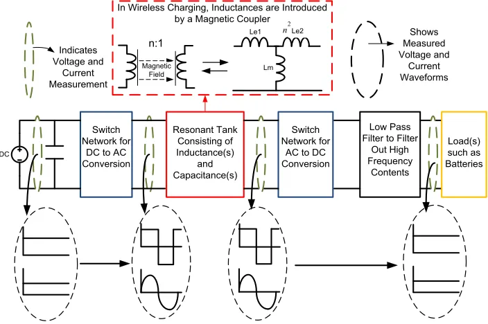
a battery or to power up an electronic load. This process is shown in Figure 1.2, which
provides a simplified overview of resonant converter operation. As Figure 1.2 shows, in
wireless charging, the DC to AC conversion generates AC signals to excite a resonant
tank whose inductances come from the T-equivalent model of a magnetic coupler,
although additional inductor(s) are sometimes implemented.
In Wireless Charging, Inductances are Introduced by a Magnetic Coupler
Switch Network for
DC to AC Conversion
Low Pass Filter to Filter
Out High Frequency
Contents DC
Switch Network for
AC to DC Conversion Resonant Tank
Consisting of Inductance(s)
and Capacitance(s)
Load(s) such as Batteries Indicates
Voltage and Current Measurement
Shows Measured Voltage and
Current Waveforms Magnetic
Field
Le1 Le2
Lm
n:1
2
n
Figure 1.2: Simplified overview of resonant converter operation.
... Equation (1)
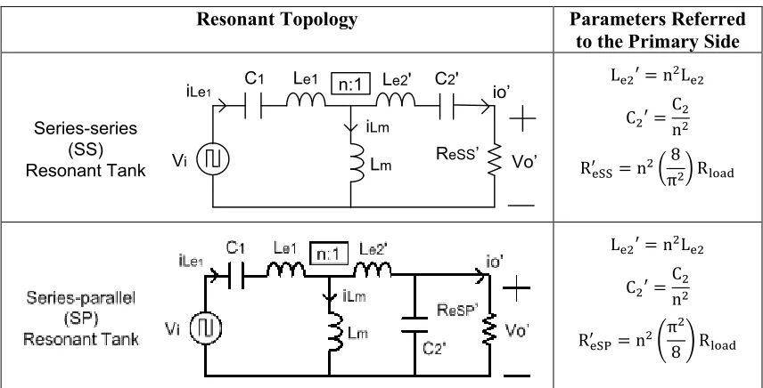
There are different possible resonant capacitor arrangements for creating various
resonant tank topologies. Two popular resonant tank topologies, series-series (SS)
resonant tank and series-parallel (SP) resonant tank, are shown in Figure 1.3- Note: Each
topology contains the T-equivalent model of the magnetic coupler, and the
secondary-side parameters are referred to the primary secondary-side. Examples of these topologies in wide
range of applications can be found in [1], [6], [8]-[9], [24], [34]-[35] and [37].
In Figure 1.3, the resonant tank input is AC voltage Vi, which is created by the
primary-side switch network performing DC to AC conversion. The resonant tank output
is represented as an effective resistive load, Re‟, referred to the primary side, which
models the secondary-side rectification network and the battery load under nominal
charging condition. The subscripts, SS and SP, are added to distinguish between the
expressions for Re' in SS and SP resonant tank topologies: ReSS‟ for SS resonant tank and
ReSP‟ for SP resonant tank. Primary-side resonant capacitance is denoted as C1, and
secondary-side resonant capacitance referred to the primary side is denoted as C2‟.
Resonant Topology Parameters Referred to the Primary Side
Figure 1.3: Series-series (SS) and series-parallel (SP) resonant tanks with secondary-side parameters referred to primary side.
C1 Le1 Le2' C2'
Lm
Vi ReSS’ Vo’
iLe1
iLm
io’
n:1
In this research, detailed analysis is performed for voltage gain ||GV(jω)||, current gain
||Gi(jω)||, and circulating current gain ||GiLm(jω)|| of the two resonant tank topologies.
Angular frequency ω is in rad/s and defined as 2πf, where frequency f is in Hz. Voltage
gain ||GV(jω)|| is defined as the magnitude of the ratio VO‟ to Vi in the frequency domain.
Current gain ||Gi(jω)|| is defined as the magnitude of the ratio of iO‟ to iLe1 in the
frequency domain. Circulating current gain ||GiLm(jω)|| is defined as the magnitude of the
ratio of iLm to iLe1 in the frequency domain.
For the two resonant tank topologies, voltage gain evaluates power transmission
characteristics. In the SS resonant tank, current gain and circulating current gain evaluate
coil-to-coil power efficiency. On the other hand, in the SP resonant tank, current gain
evaluates the resonant tank's power efficiency while circulating current gain evaluates
coil-to-coil power efficiency. This is because current gain of the SP resonant tank is
affected also by one additional circulating current path through C2‟ unlike the SS
resonant tank – See Figure 1.3.
As mentioned previously, the coupler can be implemented either asymmetrically or
symmetrically. Due to this fact, there are two main types of resonant tank that the SS
resonant tank and SP resonant tank can belong to. One is asymmetrically-implemented
resonant tank (ART) type, and the other is symmetrically-implemented resonant tank
(SRT) type. In ART type, the primary leakage (Le1) and the secondary leakage referred to
the primary side (Le2' = Le2) can be largely different, thus they are not related simply by
the coupler turns ratio, n. In SRT type, Le1 and Le2' are equal to each other. Thus, in SRT
LS1 > LS2', LS1 = LS2', or LS1 < LS2'. Consequently, analytical complexity is higher for
ART type.
These two main resonant tank types can be further divided based on the range of k.
ART type can be divided into tightly-coupled ART (TART) type or loosely-coupled ART
(LART) type. Also, SRT type can be either tightly-coupled SRT (TSRT) type or
loosely-coupled SRT (LSRT) type. In this research, the term, „tightly-loosely-coupled‟, refers to k ≥ 0.6
approximately, whereas the term, „loosely-coupled‟, corresponds to k ≤ 0.35
approximately.
1.2MOTIVATION AND RESEARCH OBJECTIVES
Wireless charging provides increased safety and convenience by applying galvanic
isolation and by eliminating the need for frequently-used dedicated connectors/adapters.
For these reasons, it has been utilized in medical implant charging [1]-[5] and electric
vehicle (EV) charging [6]-[9]. Recently, wireless charging has become an attractive
charging solution also for electronic household appliances and various portable
electronics [10]–[13] such as cellular phones [14]-[16] and laptops [17]-[18]. This is
because wireless charging can also provide aesthetically-pleasing cord-free environment
that improves spatial utilization. However, current wireless charging technology
demonstrates several shortcomings.
From the consumer‟s perspective, the shortcomings include limited receiver
positioning flexibility and lower power transmission efficiency compared to
wire-connected charging. From the industry‟s perspective, they include increased cost due to a
In order to promote adoption of wireless power transfer technology, it is crucial to
provide good efficiency in both tightly-coupled systems and loosely-coupled systems
while reducing the complexity in design optimization and control of resonant converters.
Furthermore, minimization of component count to reduce the cost of implementation is
highly desirable.
However, there exist various challenges due to the fact that significant variations can
occur in k and Re'. Variation in k is caused by the misalignment and air-gap changes
between Tx and Rx - See Figure 1.1. This variation changes the inductances (Le1, Le2',
and Lm) and thus causes resonant frequencies to shift. Variation in Re' can occur passively
and/or actively. Passive variation in Re‟ occurs due to battery state of charge variation or
due to different electronic loads. Active variation in Re‟ occurs due to various
rectification (AC to DC conversion) techniques. Both types of variation (k variation and
Re‟ variation) causes resonant peaks to change in voltage gain, current gain, and/or
circulating current gain. These resonant peak changes can be described in terms of quality
factor, Q. Expressions for Q depend on resonant tank topologies and author. In this
research, Q describes relationship between resonant elements and effective resistive load,
Re'. Therefore, Q in this research is a load-dependent quantity. Different mathematical
expressions for Q are used later in this dissertation. For now, it should be noted that Q
variation can be imposed by changing Re'. In summary, resonance characteristics of a
resonant tank can vary significantly in wireless power transfer applications.
The parameter variations affect power transmission characteristics, efficiency, and
control model complexity. More specifically, the following general remarks, a through d,
can be made regarding various affected quantities in wireless charging applications.
a. Maximizing power transmission robustness against k variation is desirable
for minimizing losses in an additional converter and/or regulator
implemented in either the transmitter-side or receiver-side of a resonant
converter. In some cases, high robustness in power transmission
characteristics can even eliminate the need for an additional converter
and/or regulator, which maximizes the overall system efficiency. It can
also significantly decrease the complexity in deriving
frequency-dependent models for controlling power transmission. Note: Power
transmission robustness is maximized when voltage gain robustness is
maximized.
b. Power efficiency in a resonant tank is maximized ideally when its leakage
inductances are fully compensated by resonant capacitor(s) to produce
effective short-circuited (zero) impedance. In a desired range of k
variation, maintaining compensation of leakage inductances provides
sufficient power delivery without significant losses in a magnetic coupler.
Therefore, there needs to be a control method that allows tracking and
achieving the compensation of leakage inductances under k variation.
c. Satisfying a through b above leads to increased receiver positioning
d. There is a trade-off between coil-to-coil power efficiency and robustness
in power delivery: high coil-to-coil efficiency of a resonant tank may be
achieved at the cost of low power delivery robustness against k variation.
This means that, under the condition that expected losses in an additional
converter and/or linear voltage regulator are higher than expected losses in
a resonant tank, it is better to increase power delivery robustness, because
overall charging system efficiency can be increased by minimizing the
losses in or the need for an additional converter and/or linear voltage
regulator.
To achieve good overall efficiency and robustness in power transmission, to improve
receiver positioning flexibility, and to reduce implementation complexity, this
dissertation presents the following novel accomplishments in order.
NOVEL ACCOMPLISHMENT 1:
To obtain a novel optimal design method for SS resonant tank of SRT type by
performing detailed analysis on frequency-domain characteristics of SS resonant
tank of SRT type.
NOVEL ACCOMPLISHMENT 2:
To obtain a novel control method that enables unity gain frequency tracking
(UGFT) in a SS resonant converter of SRT type under k variation without the
NOVEL ACCOMPLISHMENT 3:
Based on detailed analysis of general frequency-domain characteristics of SS and
SP resonant tank topologies, derive general analytical equations in
design-oriented form for determining various notable quantities in SS and SP resonant
tank topologies. By using these equations, perform analytical comparative study
on SS and SP resonant tank topologies for deciding which of the two topologies is
desirable for a certain application. Also, obtain novel computer-aided optimal
design methods, so that the two topologies of LART type can be designed for
optimal performance for a desired nominal load under k variation.
1.3RESEARCH SIGNIFICANCE
In novel accomplishment 1, frequency-domain characteristics of SS resonant tank of
SRT type are analyzed in detailed to evaluate changes in the characteristics caused by k
and Q variations. Based on the analysis, a novel design method is developed. The design
method allows rapid calculation of the resonant tank parameters for achieving peak
voltage gain of choice. As will be shown, unlike conventional design methods, it is a
more self-contained method in which the cost of design process can be significantly
reduced. By allowing rapid calculation of the resonant tank parameters, it also provides
convenient evaluation of expected resonance characteristics for SS resonant tank of SRT
type. Consequently, design iterations can be performed without high complexity and
time-consuming efforts that conventional design methods require.
In novel accomplishment 2, a novel UGFT control method is developed for SS
resonant tank of SRT type. This method does not require communication between a
power efficiency (unity voltage gain frequency, fO). Therefore, this control method can
improve both power efficiency and receiver positioning flexibility in SS resonant
converter of SRT type. By minimizing the need for various components in currently
available wireless charging systems for portable electronics, this control method also
reduces system complexity and cost of implementation.
In novel accomplishment 3, detailed analysis on general frequency-domain
characteristics of SS and SP resonant tank topologies is performed. By deriving various
general analytical equations, SS and SP resonant tank topologies of both SRT and ART
types can be analyzed. Assuming loosely-coupled condition, equations for approximating
desirable resonant frequencies under k variation are derived. Using these frequency
approximations, various design equations are derived. All of the analytical equations and
design equations are derived in design-oriented forms consisting only of
physically-meaningful quantities that allow convenient analysis and optimal designs of the two
popular resonant tank topologies. Also, these equations allow determining and evaluating
various important frequency-domain quantities such as peak voltage gain,
load-independent voltage gain, load-load-independent current gain, multiple resonant frequencies
exhibiting notable features, desirable boundary for operating frequency (ωs) range,
voltage gain at ωs, current gain at ωs, circulating current at ωs, and how these quantities
change depending on magnetic coupling coefficient (k) and load (Re‟). Therefore, easier
understanding of design and efficiency tradeoffs can be accomplished by using these
equations. By using the design equations, novel computer-aided optimal design methods
for loosely-coupled SS resonant tank and loosely-coupled SP resonant tank are developed
experimental evaluation and iterative practical redesigns. These design methods allow
rapid and convenient evaluation of effects of variations in k and load-dependent quality
factor. Optimal load-dependent quality factor values can then be determined without high
complexity for a desired nominal load. By achieving optimal load-dependent quality
factors, power transmission robustness against k variation can be maximized without
significantly reduced coil-to-coil power efficiency. Also, an analytical comparative study
is performed to show which of the two topologies is desirable for a certain application.
Overall, these novel accomplishments contribute to improving both overall power
efficiency and receiver positioning flexibility, while reducing system complexity and cost
of design process in inductive wireless charging systems.
1.4BACKGROUND ON RESONANT CONVERTERS
Unlike pulse width modulated (PWM) converters, resonant converters contain a
resonant L-C network (resonant tank) that produces sinusoidal or quasi-sinusoidal voltage
and current waveforms during a switching period.
To increase the power density, switched-mode power converters can be operated at
high switching frequencies so as to reduce the sizes of magnetic components. However
for a PWM converter performing hard switching transitions, high switching frequency
operation can increase the switching loss significantly leading to poor power efficiency.
A major advantage of resonant converters is the reduced switching loss through the
use of soft switching techniques known as zero voltage switching (ZVS) and zero current
switching (ZCS). In ZVS and ZCS, the turn-on transitions and/or turn-off transitions of
semiconductor switches can occur approximately at zero crossings of the waveforms
resonant converter, so that it can operate at switching frequencies higher than in
comparable PWM converters. Another advantage of resonant converters is that ZVS can
reduce the electromagnetic interference (EMI) by significantly reducing high frequency
noise at switching transitions.
However, there exists a major disadvantage of resonant converters: it is difficult to
optimize the resonant elements in terms of efficiency for wide input and output ranges.
Also, optimization becomes even more difficult when there are variations in k such as in
wireless power transfer applications.
In this section, the fundamental theory on resonant converters is explained: the
fundamental theory includes sinusoidal analysis, ZVS mechanism, and ZCS mechanisms.
A simple DC-DC series LC resonant converter in Figure 1.4 is used as an example to
explain the theory. Furthermore, various types (switching frequency (fS) modulation,
phase-shift method, and PWM method) for controlling the voltage gain and load current
are described.
Figure 1.4: DC-DC series LC resonant converter.
1.4.1SINUSOIDAL ANALYSIS OF RESONANT CONVERTERS
In Figure 1.4, actively controlled switches, Q1-Q4, convert a DC source voltage, Vg,
to a square wave voltage, vS(t), oscillating at the switching frequency, fS. In most cases,
the frequency of v (t) is close to the resonant frequency, f , generating the
quasi-Vg
C L
ig(t)
is(t) ir(t)
Q1
Q2
Q3
Q4
Io |ir(t)|
Vo
Vs(t) Vr(t)
sinusoidal waveforms in the resonant tank. If the resonant tank has response at other
harmonics of vS(t) that are negligible compared to response at the fundamental frequency
(fS ≈ fO), then the voltage and current waveforms of the resonant tank can be
approximated by their fundamental frequency components. Thus, the resonant tank acts
as a fundamental frequency pass filter. Applying the fundamental frequency
approximation in the analysis, vS(t) can be realized as shown in Figure 1.5. This figure
shows the square wave voltage, vS(t), which is what the input voltage of the resonant
tank actually is. Due to the filtering effect, the sinusoidal wave voltage, vS1(t), is what the
impedance of the resonant tank responds to. Using Fourier series, the square wave
voltage, vS(t), is represented by Equation 2. Since the resonant frequency, fo, is close to
the fundamental frequency, , the fundamental component of vS(t) applied to the
input of the resonant tank can be expressed as Equation 3. The quasi-sinusoidal resonant
tank input current, is(t), is then expressed as Equation 4 - Note: The phase shift, s, is
present in is(t) when fS and fO are not exactly equal to each other.
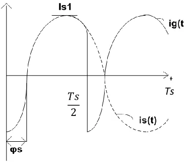
Figure 1.6 shows the source current, ig(t), and resonant tank input current, is(t),
waveforms: ig(t) and is(t) are equal for one half of the switching cycle, but they are
opposite in polarity for the other half. This can be easily understood by visualizing ig(t)
as a phase-shifted full-wave rectified version of is(t) hence ig(t) having some negative
polarity portion for duration. The average value of ig(t) is then determined by
Equation 5.
As can be seen from Figure 1.5 and Figure 1.6, is(t) is shown to lag vS(t) by the phase
shift of . This lagging occurs because the analysis performed here is based on
the resonant tank introduces an inductive impedance to for fS > fO(above-resonance
operation). On the other hand, if fS is belowfO, then is(t) is leads vS(t) by a certain phase:
with the series L-C configuration, the resonant tank introduces a capacitive impedance to
vS(t) for fS < fO(below-resonance operation). The magnitude of phase shift increases as fS
is moved farther away from fO. It should be noted that is(t) waveform is then
quasi-sinusoidal: is(t) is sinusoidal only if fS is exactly equal to fO so that the resonant tank
introduces a resistive impedance to vS(t) causing no phase shift between is(t) and vS(t) .
The portion consisting of the diode bridge rectifier, output low pass filter, and load
resistor is shown Figure 1.7. The series LC resonant tank‟s output voltage (vr(t)), its
fundamental component (vr1(t)), and output current (ir(t)) waveforms are shown in Figure
1.8.
Because of the synchronous rectification performed by the diode bridge rectifier, the
effective resistive load, Re, is applied to the output of the resonant tank as indicated in
Figure 1.7. In order to determine Re, is first represented as Equation 6, and its
fundamental component, , is then represented as Equation 7. The output current of
the resonant tank, ir(t), is expressed as Equation 8. Then, the output current through the
load resistor, Io, which is filtered by the low pass capacitive filter, Cf, is equal to the
average value of the full-wave rectified current of ir(t), |ir(t)|, which is shown by Equation
9. Finally, effective resistive load Re is derived as Equation 10.
Based on Equations 2 through 10, the steady-state equivalent model of the series LC
resonant converter is shown as Figure 1.9. The ratio of load voltage (VO) to source
voltage (Vg), M, is determined by Equation 11. Substituting Equation 10 into Equation
, because there are some losses. This relationship shows that the output
voltage of resonant converters depends on the voltage gain transfer function of the
resonant tank and can be controlled by modulating the switching frequency, fS.
Figure 1.5: Square wave resonant tank input voltage, vS(t), and its fundamental frequency
component, vS(t).
,... 7 , 5 , 3 , 1
) sin( 1 4
) (
n
st
n n Vg
t
Vs
... Equation (2)
) sin( )
sin( 4 )
( 1
1 t V t
Vg t
Vs s s s
... Equation (3)
) sin(
)
(t Is1 st s
is ... Equation (4)
Figure 1.6: Source current, ig(t), and resonant tank input current, is(t).
) (j s Gv
M
Vg
4
) cos( 2 ) sin( 2 ) ( 2 ) ( 1 2 0 1 2 0 s s Ts s s s Ts
Ts Ts ig t dt Ts I t dt I
t ig
... Equation (5)Figure 1.7: Diode bridge rectifier with low pass filter and load resistor.
Figure 1.8: Waveforms of the series LC resonant tank‟s output voltage vr(t), its
fundamental component vr1(t), and resonant tank output current ir(t).
,... 7 , 5 , 3 , 1 ) sin( 1 4 ) (n s r
t n n Vo
t
Vr
... Equation (6)
... Equation (7)
) sin(
)
(t Ir1 st r
ir ... Equation (8)
C
fVo
1 2 0 1 2 | ) sin( | 2 r Ts r s
r t dt I
I Ts Io
... Equation (9)R Io Vo t i t V r r 2 2 1
1 8 8
) ( ) ( Re
... Equation (10)
Figure 1.9: Steady-state equivalent model of series LC resonant converter.
4 ) ( 1 2 ) ( 1 1 1 1 1 1 s e s s r r r r j Gv R R Vg V V V V I I Io Io Vo Vg VoM ... Equation (11)
1.4.2ZERO VOLTAGE SWITCHING (ZVS)
ZVS is a type of soft switching mechanism that reduces the switching loss by having
switching transitions of semiconductor devices at zero crossings of applied voltage
waveforms. For example, in converters containing MOSFETs with built-in anti-parallel
body diodes or external diodes, ZVS reduces the switching loss caused by diode reverse
recovery and inherent output capacitance of a MOSFET.
ZVS can occur where the voltage across a MOSFET becomes zero before the resonant
tank current becomes zero, and before the transistor turns on. Therefore in
above-resonance operation of the series LC resonant converter in Figure 1.4 , the MOSFETs in
Q1-Q4 can turn on softly with ZVS, leading to the reduced turn-on switching losses.
(iS(t)) under ZVS. As can be seen from this figure, the soft turn-on transition occurs when
iS(t) crosses zero at t1, at which point, vS(t) is in its positive half while iS(t) is making the
polarity transition from negative to positive. In Figure 1.10, initially, iS(t) is negative
while vS(t) is positive, and the body-diodes of MOSFETs, Q1 and Q4, are conducting.
When iS(t) is at its zero crossing, t1, the MOSFETs, Q1 and Q4, turn on softly with ZVS,
because during the transition, the voltages across Q1 and Q4 are zero while the current
going through Q1 and Q4 are sinusoidally changing. This ZVS operation is more evident
in Figure 1.11 which shows the voltage, vds1(t), across Q1 and the current, ids(t), through
it.
The transistor turn-off in Figure 1.11 is a hard switching transition similar to what
transistors of PWM converters exhibit. ZVS can be achieved also for turn-off transitions
by introducing an appropriate dead time (DT), during which all of Q1-Q4 are turned off.
During this DT after the square wave resonant tank input voltage crosses zero, the
remaining charge indicated by the area under the sinusoidal current curve are exchanged
by the parallel capacitors of the transistors. After the capacitors are fully charged at the
supply voltage, the anti-parallel diodes clamp at this voltage as seen in Figure 1.11 and
these diodes allow conduction of free-wheeling diode current to circulate into the parallel
capacitors, thus introducing commutation intervals. During the commutation intervals,
the transistor voltages change softly due to charging and discharging of their parallel
capacitors. When this happens, both the rising and falling edges of the transistor voltage
Figure 1.10: ZVS during turn-on transitions of MOSFETs in series LC resonant converter of Figure 1.4 in above-resonance operation.
Conducting Devices: D1D4
Q1 Q4
D2 D3
Q2 Q3
Ts/2 Ts t
t1 is(t)
Vs1(t)
Vs(t) Vg
-Vg
Soft turn-on
of Q1 and Q4
Hard turn-off of Q1 and Q4
Soft turn-on
of Q2 and Q3
Hard turn-off of Q2 and Q3
Figure 1.11: MOSFET Q1 voltage and current of series LC resonant converter in above-resonance operation for ZVS.
Figure 1.12: Introduction of commutation interval, X, where charging and discharging of parallel capacitors of transistors occur for soft transistor voltage transitions.
Conducting
Devices: D1D4 Q1Q4
D2 D3
Q2 Q3
Ts/2 Ts t
t1 ids(t)
Vg
Soft turn-on
of Q1 and Q4
Hard turn-off
of Q1 and Q4
Soft turn-on
of Q2 and Q3
Hard turn-off
of Q2 and Q3
Vds1(t)
t
Conducting Devices:
Q1 Q4
D2 D3
Q2 Q3 Vg
Soft turn-on
of Q1 and Q4
Soft turn-on
of Q2 and Q3
Vds1(t)
t X
Soft turn-off
1.4.3ZERO CURRENT SWITCHING (ZCS)
As mentioned previously, when the series LC resonant converter in Figure 1.4 is
operated at fS < fO (below-resonance operation), the series LC resonant tank has a
capacitive input impedance. In this case, is(t) leads vS(t)as shown in Figure 1.13. Then,
the transistor current crosses zero before the transistor voltage becomes zero, thus
achieving ZCS. Figure 1.14 shows this phenomenon using the vds1(t) and ids(t) of Q1.
Figure 1.13: ZCS during turn-on transitions of MOSFETs in series LC resonant converter of Figure 1.4 in above-resonance operation.
Conducting
Devices: Q1Q4 D1D4 Q2Q3 D2D3
Ts/2 Ts/2+tb
tb
is(t)
Vs1(t)
Vs(t) Vg
-Vg
Soft turn-off
of Q1 and Q4 Hard
turn-on of Q1 and Q4
Hard turn-on of Q2 and Q3
Soft turn-off
Figure 1.14: MOSFET Q1 voltage and current of series LC resonant converter in below-resonance operation for ZCS.
1.4.4CONTROL OF OUTPUT POWER DELIVERY VIA SWITCHING FREQUENCY MODULATION
As briefly described previously, the voltage gain of a resonant converter depends on
switching frequency. The series LC resonant tank in Figure 1.4 exhibit the voltage gain
transfer function of Equation 12. This equation shows that the highest voltage gain
possible for the series LC resonant tank is unity at the resonant frequency, . As
the switching frequency, fS, moves away from fO, the voltage gain decreases. This is
expected because the impedances of L and C cancel each other when fS = fO, causing the
resonant tank input voltage to be applied directly across Re. So, the limitation of the
D1 D4 Q1
Q4
D2 D3 Q2
Q3
Ts/2 Ts t
tb
ids(t)
Vg
Soft turn-off
of Q1 and Q4 Hard
turn-on of Q1 and Q4
Hard turn-on of Q2 and Q3
Soft turn-off
of Q2 and Q3
Vds1(t)
t
Conducting Devices:
series LC resonant tank is that it can operate only for a voltage step-down conversion
(buck mode).
However when the inductor is replaced with a magnetic coupler, the highest voltage
gain available, ||GV||max, can exceed unity for boost mode operation even when the turns
ratio of unity is applied for primary coil and secondary coil. This is possible due to the
parallel path introduced by a magnetizing inductance, Lm. Detailed analysis is performed
in later chapters clearly showing this property among other important frequency-domain
characteristics. For now, it should be noted that the output voltage of a resonant tank can
be controlled by varying the transistor switching frequency, fS.
, where and ... Equation (12)
1.4.5CONTROL OF OUTPUT POWER DELIVERY VIA PULSE WIDTH MODULATION
In DC-DC resonant converters, using fully-controllable switches for active
rectification rather than using a diode-bridge rectifier allows flexible control of the load
current. It also reduces the diode conduction loss. In low power applications, the forward
diode voltage drop and diode current can cause a significant efficiency loss; therefore
fully-controllable switches should be used as synchronous rectifiers rather than diodes.
Implementation of fully-controllable switches on both sides of a magnetic coupler
produces a bidirectional DC-DC resonant converter in which power delivery can be
controlled by methods other than the switching frequency modulation technique. One of
the methods is pulse width modulation (PWM) technique that varies the duration in
which switches are turned on. An example of PWM technique is explained using the
quantities indicated in the fully-controllable full-bridge rectifier of Figure 1.15. 2 1 ) ( o o e o e j Q j Q j j Gv
o LC
1 Re C L
In the PWM technique, the duty cycle of a resonant tank‟s output voltage, Vr(t), can
be controlled as shown in Figure 1.16. The load current, Io, is then represented as
Equation 13, which shows that Io can be changed by varying the duty cycle - Note: the
change in the parameter, n, represents the duty cycle variation (on-off time variations of
the secondary-side switches).
It should be noted that the PWM technique can be performed also on the primary side,
varying the on-off time of the primary-side switches. The maximum power delivery
occurs when the duty cycle is 50 % as can be seen from Equation 13: the parameter, n,
has to be a very high number (mathematically, infinity), causing both the negative portion
and positive portion of ir(t) to be half of switching period, Ts. Therefore, any deviation
from 50% in duty cycle condition (on-off time variation) results in decreasing theoutput
power (load current, Io) only, providing a limited control capability.
Figure 1.15: Fully-controllable full-bridge rectifier.
Q8 Q6
Q7 Q5
R
Vo
|ir(t)|
ir(t) Cf
Io
D5
D6
D7
D8
Figure 1.16: PWM technique for controlling resonant tank output power via active on-time variation of the switches in the secondary-side full-bridge rectifier.
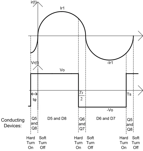
where ... Equation (13)
1.4.6CONTROL OF OUTPUT POWER DELIVERY VIA PHASE SHIFT METHOD
Another method of controlling the power delivery can be achieved with the
requirement of using fully-controllable switches both on the primary side and secondary
side. The method is called phase shift method and applies either an inductive phase shift
or a capacitive phase shift to decrease the load current.
When an inductive phase shift is applied actively, Vr(t) waveform leads ir(t)
waveform as in Figure 1.17. The load current is then expressed as Equation 14, which
t |ir(t)| Vr(t) ir(t) Vo -Vo Ir1 Ir1 Ir1 -Ir1 Conducting Devices: D5 or Q5
shows that the load current can be controlled by varying the phase shift, -Note: the
maximum power delivery occurs when .
When a capacitive phase shift is applied actively, Vr(t) waveform lags ir(t) waveform
as in Figure 1.18. The load current is then controlled again by controlling the phase shift,
.
In summary, besides the switching frequency (fS) modulation technique, the PWM
technique and/or the phase shift technique can be used to control the power delivery (load
current, Io). It is shown in Figure 1.16 through Figure 1.18 that these two methods
introduce actively controlled effective load condition to a resonant tank. It will be shown
later in Chapter 4 that both the PWM technique and the phase shift technique are
undesirable in terms of control complexity and efficiency. On the other hand, fS
modulation technique is desirable.
Vr(t) ir(t)
Vo
-Vo Ir1
-Ir1
Conducting Devices:
Q5 and Q8
D5 and D8 Q6 and Q7
D6 and D7 Q5 and
Q8
t
tφ 2
Ts Ts
Hard Turn On
Soft Turn Off
Hard Turn On
Soft Turn Off
Hard Turn On
where
... Equation (14)
Figure 1.18: Phase-shift control to apply capacitive effective load.
1.5THEORY OF OPERATION OF SSRESONANT CONVERTER OF SRTTYPE
The purpose of this section is to describe the ideal operation of a SS resonant
converter of SRT type in wireless charging applications. Figure 1.19 shows a DC-DC
full-bridge-to-full-bridge SS resonant converter of SRT type. For the sake of simple
discussion, 1:1 turns ratio is also applied for coupler winding condition. This means that
Le1 = Le2 = Le2', and consequently leakage inductance compensation is achieved by Cr: C1
= C2 = C2'. The winding resistances and core loss resistance model are not included in the
T-equivalent model.
Vr(t) ir(t)
Vo
-Vo Ir1
-Ir1
Conducting Devices:
D5 and D8 andQ6
Q7 D6 and D7 Q5
and Q8
t
tφ 2
Ts Ts
Hard Turn Off Soft Turn On
Soft Turn On
Hard Turn Off Hard
Figure 1.19: DC-DC bidirectional full-bridge SS resonant converter of SRT type.
1.5.1THEORETICAL WAVEFORMS UNDER IDEAL SWITCHING TRANSITIONS ON PRIMARY SIDE
In Figure 1.20, various waveforms of the SS resonant converter in Figure 1.19 are
shown to describe the nominal, ideal converter operation for each switching interval.
Constant input and resistive load conditions are assumed with a DC input voltage source
and load resistor. The nominal, ideal operation is when the switching frequency (fS) is
equal to the unity gain resonant frequency, fO (Equation 15).
At fS = fO, the impedances of Cr-Le1 and Cr-Le2 branches are effectively shorted as
mentioned before. The SS resonant tank can then be represented by the simplified
equivalent model in Figure 1.21. Therefore, the resonant tank driving-square wave
voltage, VH1(t), is directly applied across Lm, causing the circulating current, iLm(t) to be
triangular rather than sinusoidal. Consequently, the voltage gain of the SS resonant tank
is unity regardless of the effective resistive load (Re') while the circulating current is
reduced leading to higher coupler efficiency.
It should be noted that in Figure 1.20, iLe1(t) is shown to lag VH1 by t , meaning that
the SS resonant tank is behaving as an inductive impedance applied to the primary-side
full-bridge, and therefore the converter is assumed to be operating under the above-Vg
Cr
VH1(t)
D1
Q1 Q3
Q2 Q4
D3
D2 D4
Vds1(t)
iLe1(t)
ig(t)
Cr
Q8 Q6
Q7 Q5
1:1
R Vo
iLe2(t)
VH2(t)
Cf1 Cf2
Le1 Le2
Lm Vds3(t)
Vds2(t) Vds4(t)
Io
Inductive Coupler with Turns Ratio of 1:1