Systematic Design of an Approximate Adder:
The Optimized Lower Part Constant –Or
Adder
A.Bhuvana, S.Jeya Anusuya, G.Bhavani,
Department of Electronics and Communication Engineering, T.J.S Engineering College, Peruvoyal, India
HOD, Department of Electronics and Communication Engineering, T.J.S Engineering College, Peruvoyal, India
Assistant Professor, Department of Electronics and Communication Engineering, T.J.S Engineering College,
Peruvoyal, India
ABSTRACT: Adders are vastly implemented in the critical path of many blocks of microprocessor chips. They are not only used in the arithmetic logic units (ALUs) but also in other parts of the processor where they are used to calculate addresses, table indices, and similar operations. The efficiency of the digital system is greatly influenced by the performance of these adders. In this paper, we proposed a low-power yet high speed accuracy- configurable adder that also maintains a small design area. The proposed adder is based on the conventional carry look-ahead adder, and its configurability of accuracy is realized by masking the carry propagation at runtime. Compared with the conventional carry look-ahead adder, the proposed 16-bit adder reduced power consumption and critical path delay most according to the accuracy configuration settings, respectively. Furthermore, compared with other previously studied adders, the experimental results demonstrate that the proposed adder achieved the original purpose of optimizing both power and speed simultaneously without reducing the accuracy.
KEYWORDS: Full adder, ALU, OR, carry propagation, carry look-ahead adder.
I. INTRODUCTION
The central component of semiconductor electronics is the integrated circuit (IC), which combines the basic elements of electronic circuits - such as transistors, diodes, capacitors, resistors and inductors - on one semiconductor substrate. The two most important elements of silicon electronics are transistors and memory devices. For logic applications MOSFETs (Metal Oxide Semiconductor Field Effect Transistor) are used. MOSFETs have been the major device for ICs over the past two decades. With technology advancement and the high scalability of the device structure, silicon MOSFET-based VLSI circuits have continually delivered performance gain and/or cost reduction to semiconductor chips for data processing and memory functions. The reduction in cost-per-function has been steadily increasing the economic productivity with every new technology generation. As the CMOS technology scaling enters the nano meter control, many serious problems called the small geometry effects or short channel effects(SCEs) comes into play. Some of these effects are such as increased leakage currents, difficulty on increase of on-current, large parameter variations, low reliability and yield, increase in manufacturing cost, and etc. In order to sustain the historical improvements, future technology scaling and to mitigate these small geometry effects to a considerable level, several strategies and new device structures have been researched and introduced. These nano-scale devices have a significant potential to
revolutionize the fabrication and integration of electronic systems and scale beyond the perceived scaling limitations of traditional CMOS.
II. LOGIC DESIGN IN ADDER
A) High-Speed Configurable Adder
Adder Circuits are the most basic block of any digital system. In any arithmetic function addition plays a role of most fundamental operation. Adders are commonly used in miscellaneous application in modern VLSI system like multiplier design, design of an ALU, and also in various Digital Signal Processing algorithms like FIR, IIR Filter design. Designing an excellent and efficient of an adder circuit a designer must optimize the parameters like area, delay, and power. We have to trade-off between all three parameters to get an efficient design. Depending upon the need and application some changes and compromises have to be made. In modern VLSI design era delay in data path considered as a crucial parameter these days. Designers are trying to minimize the delay as the speed up operation becomes faster. There has been lot of researches and work regarding minimizing of delay and now designer look for making an adder circuit which is efficient and significantly faster.
Few basic adders like Ripple carry adder, Carry Save Adder, Carry look-ahead Adder, Carry Select Adder & Kogge stone adder have been briefly explained.
B) Ripple Carry Adder
Ripple Carry Adder (RCA) is considered as the most Simplistic approach among all the addition algorithms. A N- bit Ripple Carry Adder requires N number of full adders. It is basically a Cascading formation of full adders in series. As a full adder block process three inputs along with carry bit and produce two outputs i.e. Sum bit and Carry-out Bits, the Carry of one full adder block acting as a carry in for the next full adder.
Fig.1 Block Diagram of 4 bit Ripple carry adder
C) Carry save Adder
Another Algorithm for faster calculation of Addition is Carry Save Adder. It is also same as full Adder. From the two inputs we first produce two temporary Outputs named as Sum and Carry. For getting sum bit we first perform bitwise XOR and for the Carry bit we execute bitwise AND for the two input numbers. And then finally add them by shifting Carry bit left by one place to Sum bit up to produce final answer.
D) Carry Look Ahead Adder
Another fast addition topology is Carry Look Ahead Adder. The main advantage of Carry Look Ahead Adder over Ripple Carry Adder is it improves the speed of operation by reducing the time needed to determine the carry bits. Carry Look Ahead adder calculate the sum and carry simultaneously by using a separate carry generation unit.
Fig .3 Working of Carry Look Ahead Adder (CLA)
E) Carry Look Ahead Adder
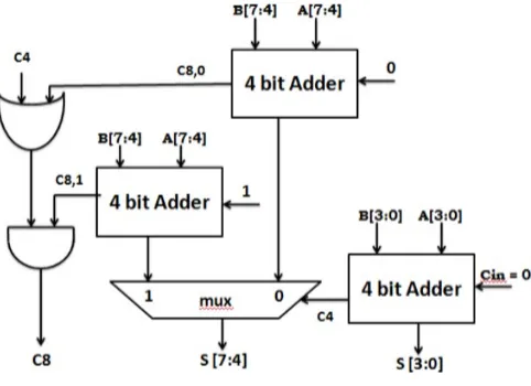
Carry Select Adder algorithm is nothing but calculating sum by guessing the carry input which we will be getting from previous stage. The diagram for this is shown below.
Fig.4 Working of Carry Select Adder (CSLA)
Two adder work simultaneously in this adder algorithms where one is calculating sum by taking carry input as 0 from the previous stage and the other adder does so by taking Carry bit as 1Several multiplexer is used to choose the appropriate sum bit corresponding to its previous carry out bit.
F) Kogge Stone Adder
generation signals are generated. Carry Generation Stage includes several Black Cells and Grey cells which used to generate carry for the next stages and finally Post-processing Stage is used to generate Sum and carry out bit.
Fig.4 Working of Kogge-Stone dder (KSA)
From the pre-processing stage we get P (a,b) and G(a,b) signals. P (a, b) = A ^ B G (a, b) = A.
From the Carry Generation Stage we get the Black cell and Grey Cells. The equations for those are
G black = (Gprev. P) + G
P black = (P. Pprev G grey = (Gprev. P) + G
Sum and Carry out bit is generated in the Post-Processing Stage. Sn = (Pn ^ Cn-1)
Kogge stone adder is one well known faster addition technique and also has a lower fan-out at the output which increases its performance but on the other hand, it occupies much area and creates wiring congestion problem.
III. EXISTING METHOD
In order to obtain the optimal architecture out of the general template, we need to evaluate all the possible combinations of 2-to-1 and 2-to-2 logic block The errors in the upper bits have a higher weight than in the lower ones. Thus, it is more profitable to expend resources in the 2-to-2 block than in the lower 2-to-1 blocks. The best 2-to-2 blocks are the OR_AND and half adder.
Fig.5 Structure of LOCA; nl =ncte +nor.
Replacing the half adder with an OR_AND does not improve the delay and improves the area only marginally; the penalty is a large increase in the MSE. For this reason, the idea of LOA (to use the OR_AND for the 2-to-2 block) is not efficient. Once we fix the 2-to-2 block to a half adder, we can observe that the average error introduced by the 2-to-2 block is zero or positive, while the 2-to-2-to-1 blocks introduce a zero or negative average error.
As an instance, a 16-bit approximate adder implemented with the OLOCA approach slightly improves MSE while reducing the ADP at the same time, in comparison with an approximate adder implemented with the LOA approach.
IV. DISADVANTAGES
It exploits the gap between the level of accuracy required by the applications and that provided by the computing system, for achieving diverse optimizations.
Uses the idea of template but is not optimal.
V. PROPOSED METHOD
In this paper, we propose a configurable approximate adder, which consumes lesser power than does with a comparable delay and area. In addition, the delay observed with the proposed adder is much smaller than that of with comparable power consumption. Our primary contribution is that, to achieve accuracy configurability the proposed adder achieved the optimization of power and delay simultaneously and with no bias toward either. We implemented the proposed adder, the conventional carry look-ahead adder (CLA), and the ripple carry adder (RCA) in Verilog HDL using a 45-nm library.Then we evaluated the power consumption, critical path delay and design area for each of these implementations. We provided a crosswise comparison to demonstrate the superiority of the proposed adder. Moreover, we implemented two previously studied configurable adders to evaluate power consumption, critical path delay Using Tanner EDA tool.
A) PROPOSEDACCURACY-CONFIGURABLE ADDER Typically, a CLA consists of three parts: (1) half
an n-bit CLA; each part of it can be obtained as follows:
Pi = Ai Bi , Gi = Ai.Bi → (1) Ci = Gi + Pi.Ci-1 → (2) Si = Pi Ci-1 → (3)
where i is denoted the bit position from the least significant bit. Note that owing to reuse of the circuit of Ai XOR B i for Si generation, here Pi is defined as Ai XOR Bi instead of Ai OR Bi. Because C0 is equal to G0, if G0 is 0, C0 will be 0. From (2), we find that C1 is equal to G1 when C0 is 0. In other words, if G0 and G1 are equal to 0, C0 and C1 will be 0. By expanding the above to i , Ci will be 0 when G0, G1, … , Gi are all 0. This means that the carry propagation from C0 to Ci is masked. From (3), we can obtain that Si is equal to Pi when Ci-1 is 0.
From the perspective of approximate computing, if G is controllable and can be controlled to be 0, the carry propagation will be masked and S (=P) can be considered as an approximate sum. In other words, we can obtain the selectivity of S between the accurate and approximate sum if we can control G to be A AND B or 0. Evidently, we can achieve selectivity by adding a select signal. Figure .7.1(a) is a conventional half adder and Fig. 7.1(b) is a half adder to which the select signal has been added. Compared with the conventional half adder, we add a signal named “M_X” as the select signal and use a 3-input AND gate to replace the 2- input one. When M_X = 1, the function of G is the same as that of a conventional half adder; when M_X = 0, G is equal to 0. AND gate. An equivalent circuit of the conventional half adder is shown in Fig. 2. This is called a carry-maskable half adder (CMHA). The dashed frame represents the equivalent circuit of a 2-input XOR (M_X = 1). We can obtain the following: P is equal to A XOR B, and G is equal to A AND B when M_X = 1; when M_X = 0, P is equal to A OR B and G is 0. Thus, M_X can be considered as a carry mask signal.
Fig.6 (a) An accurate half adder, and (b) a half adder with a select signal.
Consider an bit CLA, whose half adders for G and P signals preparation are replaced by CMHAs. In this case, an n-bit carry mask signal for each CMHA is required. To simplify the structure for masking carry propagation, we group four CMHAs and use a 1-bit mask signal to mask the carry propagation of the CMHAs in each group. The structure of a group with four CMHAs is shown in Fig. 7.3 as an example. A30, B3-0, P3-0, and G3-0 are 4-bit-length signals and represent {A3, A2, A1, A0}, {B3, B2, B1, B0}, {P3, P2, P1,
P0}, and {G3, G2, G1, G0,}, respectively. M_X0 is a 1-bit signal and is connected to the four CMHAs to mask the carry propagation simultaneously. When M_X0 = 1, P3-0 = A3-0 XOR B3-0, and G3-0 = A3-0 AND B30; when M_X0 = 0, P3-
Consider the condition when the inputs Ai and Bi are both 1, when M_Xi = 1, the accurate sum Si and carry Ci will be 0 and 1 ({Ci , Si} = {1,0}); when M_X0 , M_X1 , … , M_Xi are all 0, Si is equal to Pi (= Ai XOR Bi = 0) as an approximate sum and Ci is equal to 0 ({Ci , Si} = {0, 0}) as discussed above. Here {,} denotes concatenation. This means that the difference between the accurate and approximate sum is 2. Toward better accuracy results for the approximate sum, we use an OR function instead of an XOR function for P generation when M_X = 0. Thus, the difference will be reduced to 1. A 2-input XOR gate can be implemented by using a 2-input NAND gate, a 2-input OR gate, and a 2-input
Fig.7 A carry-maskable half adder
Fig.8 Structure of a group with four CMHAs.
mask signal for CMHA15-12 in this example; therefore, accurate P15-12 (= A15-12 XOR B15-12) and G15-12 (=A15-12 AND B15-12) are always obtained. P15-0 and G15-0 are the outputs from Part 1 and are connected to Part 2. Note that P15-0 is also connected to Part 3 for sum generation. In Part 2, four 4-bit carry look-ahead units (unit 0, 1, 2, 3) generate four PGs (PG0, PG1, PG2, and PG3), four GGs (GG0, GG1, GG2, and GG3), and 12 carries (C2-0, C64, C10- 8, and C14-12) first, and then the carry look-ahead unit 4 generates the remaining four carries (C3, C7, C11, and C15) by using the PGs and GGs. C15-0 is the output of Part 2 and is connected to Part 3. The fifteen 2-input XOR gates in Part 3 generate the sum.
The structure of the proposed 16-bit adder is shown in Fig. 4 as an example. Four groups (CMHA3-0, CMHA7-4, CMHA118, and CMHA15-12) are used to prepare the P and G signals. Each group comprises four CMHAs There is no ADVANTAGES
Optimal Operation of Adder result.
Considerable improvement in both error and hardware cost metrics
Improves MSE by 58% while reducing the ADP by 13.8%
VI. CONCLUSION
In this paper, an accuracy-configurable adder without suffering the cost of the increase in power or in delay for configurability was proposed. The proposed adder is based on the conventional CLA, and its configurability of accuracy is realized by masking the carry propagation at runtime.
REFERENCES
[1]. Najafi, M. Weißbrich, G. P. Vayá, and A. Garcia- Ortiz, “A fair comparison of adders in stochastic regime,” in Proc. 27th Int. Symp. Power Timing Modeling, Optim. Simulation (PATMOS), Sep. 2017, pp. 1–6.
[2]. S. Mittal, “A survey of techniques for approximate computing,” ACM Comput. Surv., vol. 48, no. 4, pp. 62-1–62-33, Mar. 2016.
[3]. C. Lin, Y. M. Yang, and C. C. Lin, “High- performance low-power carry speculative addition with variable latency,” IEEE Trans. Very Large Scale Integr. (VLSI) Syst., vol. 23, no. 9, pp. 1591– 1603, Sep. 2015.
[4]. V. Gupta, D. Mohapatra, A. Raghunathan, and K. Roy, “Low-power digital signal processing using approximate adders,” IEEE Trans. Comput.- Aided Design Integr. Circuits Syst., vol. 32, no. 1, pp. 124– 137, Jan. 2013.