High Selectivity Differential Bandpass Filter Using
Dual-Behavior Resonators
Xin Gao, Wenjie Feng*, and Wenquan Che
Abstract—A high selectivity differential bandpass filter (BPF) using two pairs of dual-behavior resonators (DBRs) is proposed in this letter. A high selectivity passband for the differential mode with second harmonic suppression is achieved, by utilizing shorted coupled lines with two short stubs. For the commonmode (CM) circuit, the CM responses can be suppressed over a wide frequency band by the loaded open/shorted stubs. To validate the feasibility of the proposed filter, a planar differential BPF (3-dB fractional bandwidth 4.9%) with good CM suppression is designed and fabricated. The theoretical and measured results agree well and show good in-band filtering performances and out-of-band harmonic suppression performances.
1. INTRODUCTION
Differential circuits have played an important role in modern wireless communication systems, due to their relatively high immunity to environmental noise, interference and crosstalk between different elements. Among various differential circuits, differential filter as a basic component occupies a pivotal position. Recently, many different differential filters with desired differential-mode (DM) frequency responses and common-mode (CM) suppression have been demonstrated [1–7]. In [1], the double-sided parallel-strip line (DSPSL) dual-mode resonator was adopted to design the narrow differential BPF. However, the upper stopband for the DM operation is a little narrow and CM suppression is not so good. In addition, various coupling structures were used to design differential BPFs, such as coupled lines [2] and coupled resonators [3]. However, the design and analysis of the coupling structures are a little complex. An S-shaped complementary split ring resonator [4] and open complementary split ring resonators [5] were also used to realize good CM suppression in the passband, respectively, but the out-of-band suppression of CM signal is not good. In addition, the wideband differential filters were implemented by T-shaped structure with open/shorted stubs in [6], or stepped- impedance resonators (SIRs) in [7].
The dual-behavior resonator (DBR) has been widely used in single/dual/tri-band filters [8–10] and duplexers [11, 12] with multiple transmission zeros. However, little research has described the application of the DBR in the differential filters. In this work, a novel high selectivity differential bandpass filter using two pairs of DBRs is proposed. Four controllable transmission zeros without complex coupling structures are introduced to suppress spurious resonances of both sides of the bandpass responses for
the DM and the upper stopband can be extended to 2.78f0. Wideband CM suppression can be also
realized by using the all-bandstop transmission characteristic of the coupling circuit. For demonstration, a prototype of the differential bandpass filter operating at 2.45 GHz is constructed on the dielectric substrate Rogers 5880 with εr = 2.2,h= 0.508 mm, and tanδ= 0.0009.
Received 7 April 2015, Accepted 21 May 2015, Scheduled 22 May 2015
* Corresponding author: Wenjie Feng ([email protected]).
2. PROPOSED DIFFERENTIAL BPF USING DBRS
Figure 1(a) shows the ideal circuit of the proposed differential BPF which consists of two pairs of DBRs with two open/shorted stubs (θ3, θ4, Z3, Z4). The pair of DBRs is composed of two side-coupled
shorted lines (θ1,Z1, even/odd-mode characteristic impedanceZoe,Zoo) and two pairs of transmission
lines (θ2, θ5, Z2, Z1). The four-port filter is ideally symmetric with respect to the central plane in
horizon (dotted-line). The equivalent half circuits of the DM/CM can be used for theoretical analysis conveniently [13] as shown in Figures 1(b) and (c).
2.1. Differential/Common Mode Analysis
When the DM signals are excited from Ports 1 and 1 in Figure 1(a), a virtual short appears along the
symmetric line, as shown in Figure 1(b). The input admittanceYin1 and the external quality factor Qe
of Figure 1(b) can be written as [14]:
Yin1=−jcot (θ1+θ5)/Z1−jcotθ2/Z2 (1)
Qe= 0.5RL(θ1+θ5) csc2(θ1+θ5)/Z1+θ2csc2θ2/Z2
(2)
AndRL is the load impedance forZ1 and Z2. As discussed in [14], the desired transmission zeros can
be easily obtained when θ1+θ5 equals to π. When Yin1 = 0, the resonant condition of two shorted
stubs can be obtained, and the external quality factor Qe of the bandpass filter can be selected from
the required value of filter specification, then the two unknown variables θ1+θ5 and θ2 can be solved
when the ratio of Z1/Z2 is fixed, in which additional impedance transformer can be avoided [14].
The simulated frequency responses of Figure 1(b) are shown in Figures 2(a)–(b). The bandwidth of DM increases as kincreases (k= (ZoeZoo)/(Zoe+Zoo)). To realize strong coupling of the side-coupled lines for the passband, here we choose Z1 > Z2. Obviously, two transmission zeros (ftz1, ftz2) are
realized by the shorted stub (θ1, Z1), and another two transmission zeros (fctz1, fctz2) are obtained
by the bandstop transmission characteristic of the side-coupled lines. Moreover, the frequencies of
ftz1, ftz2 decrease as the electrical length (θ1) of shorted stubs increases when the ratio of Z1/Z2 is
fixed. Meanwhile Qe increases as θ1 increases. In addition, θ5 has a great influence on the out-of-band
suppression. Due to the electrical length of the side-coupled lines is stillθ1, the two transmission zeros
(fctz1,fctz2) do not change.
2Z3 2Z4
θ3 θ4
Zo
Zo
Zoe
Zoo
Z1 Z1,θ5
θ1
Z2
θ2
Z1,θ5
Z2
θ2
1 2
Zo
1 2
Zo
Zoe
Zoo
Z1 Z1,θ5
θ1
Z2
θ2
Z1,θ5
Z2
θ2
Zo
1 2
Zo
Zoe
Zoo
Z1 Z1,θ5
θ1
Zo
2' 1'
Zo
Zoe
Zoo Z1
θ1 Z2
θ2
Z1 ,θ5 Z1,θ5
Z1,θ5
Z2
θ2 Z2
θ2
Z2
θ2
Symmetric line
Z3,θ3 Z4,θ4
(a)
(b) (c)
157 158 159 160 161 1.4 1.6 1.8 2.0 2.2 2.4 2.6 Qe ftz2 ftz1 Q e f , f (GHz) tz 1 tz 2
θ (deg)
Z =107 1 Ω, Z =55 Ω2 Z =117 1 Ω, Z =65 Ω2 Z =127 1 Ω, Z =75 Ω2
10 20 30 40 50 60 70 ftz2 ftz1 fctz2 |S | (dB) dd 21 Frequency (GHz)
θ =8 fctz1
o 5
θ =13o 5
θ =18o 5 -80 -60 -40 -20 0 1
1 2 3 4 5 6
(a) (b)
Figure 2. Simulated frequency responses of the differential mode of Figure 1(b), (a) versusθ1,θ5= 13◦,
(b) versus θ5, θ1 = 159◦,θ2 = 13◦, Z1 = 117 Ω, Zoe = 147.6 Ω, Zoo = 75.8 Ω, Z2 = 65 Ω, (Zo = 50 Ω, f = 2.45 GHz).
-80 -60 -40 -20 0 |S | (dB) cc 21
θ =45o 4 θ =51o
4 θ =57o
4 1 3 Frequency (GHz) 6 5 4 2
Figure 3. Simulated frequency responses of the common mode of Figure 1(c) versus θ4, θ1 = 159◦,
θ2= 13◦,θ5= 13◦,Zo = 50 Ω,Z1 = 117 Ω,Z2 = 65 Ω,f = 2.45 GHz.
When the CM signals are excited from Ports 1 and 1 in Figure 1(a), a virtual open appears along
the symmetric line, as shown in Figure 1(c). According to the preceding description, the CM operation circuit is based on the allstop transmission characteristic of the side-coupled lines with open loaded
stubs. However, the open stub (θ2, Z2) causes a harmonic response. To eliminate the impact, two
open/shorted stubs (θ3, θ4, Z3, Z4) are introduced to suppress the response. For the common mode,
the input impedanceZin2 can be written as:
Yin2=−jcot(θ1+θ5)/Z1+j
Z2+ 2Z4cotθ4tanθ2
2Z2Z4cotθ4−Z22tanθ2
(3)
WhenZin2 = 1/Yin2= 0, the transmission zero occurs at the center frequency. As we can see, good CM
suppression in a wide band can be obtained by properly choosingθ4, as shown in Figure 3. Meanwhile,
the shorted stub (θ3,Z3) only has a little effect on the harmonic suppression. In this way, a differential
filter with high selectivity and wideband CM suppression can be easily realized.
2.2. Proposed Differential Bandpass Filter
To demonstrate the proposed concepts, an experimental Chebyshev bandpass filter is implemented with fraction bandwidths of 4.9%. Based on the required responses, the lumped element values of the second-order prototype filter are determined as follows: g0 = 1, g1 = 1.4029, g2 = 0.7071, g3 = 1.9841. The
required coupling coefficient and the external quality factor can be obtained based on [15]
Qe=g0g1/F BW, k=F BW/
It can be calculated that Qe = 28.6 and k = 0.049. The Qe factor and the coupling coefficient are extracted based on [15]
Qe=f0/Δf±90◦, k=
f22−f12/f22+f12 (5)
where f is the resonant frequency and Δf±90◦ the bandwidth over which the phase shifts ±90◦ with
respect to the absolute phase at f0, and f1 and f2 are the two resonant frequencies of the shorted
coupled lines. First of all, choose the desired center frequencyf0 of the differential mode, and according
to (1)–(2), choose the properQeand ratio ofZ1/Z2to obtain the desiredθ1+θ5andθ2. And then adjust
coupling gap (g) andθ1 to realize better transmission characteristic for the differential mode. Finally,
optimize the two open/shorted stubs (θ3, θ4, Z3, Z4) to maximize the common mode suppression.
Based on the above theoretical analysis, the final parameters for the proposed differential BPF circuit of Figure 1(a) are given below: Z0= 50 Ω, Z1 = 117 Ω, Z2 = 65 Ω,Z3= 30 Ω, Z4 = 19 Ω, Zoe= 141 Ω, Zoo = 84 Ω, θ1 = 162◦, θ2 = 14◦, θ3 = 40◦, θ4 = 56◦, θ5 = 15◦, f0 = 2.45 GHz. Figure 4 shows the
top view and photograph of the proposed differential BPF. The simulated results are shown in Figure 5 (Ansoft HFSS v.13). For the DM, a second-order passband with 3-dB bandwidth 5.2% (2.35–2.48 GHz) is realized. The insertion loss (|Sdd21|) is less than 0.7 dB while the return loss (|Sdd11|) is over 18 dB
at f0. Four transmission zeros are found to locate at 1.62 GHz 2.67 GHz, 4.78 GHz and 5.18 GHz.
Furthermore, over 18-dB upper stopband is obtained (2.54–6.14 GHz, 2.5f0). For the CM, the insertion
loss (|Scc21|) is greater than 15 dB (0–5.5 GHz, 2.25f0).
Figure 4. Top view and photograph of the differential BPF (L1= 28 mm,L1 = 11.9 mm,L2 = 6.8 mm,
L3 = 10 mm, L4 = 14 mm, L5 = 3.7 mm, W0 = 1.53 mm, W1 = 0.3 mm, W2 = 1 mm, W3 = 3.1 mm,
W4= 5.3 mm,d= 0.6 mm, g= 0.3 mm, S= 2.63 mm, 34 mm×67 mm).
2.2 2.4 2.6
2.6f0
-18 dB
| S | |S |
Frequency (GHz)
Measurement Simulation
|S |
|S |
Frequency (GHz)
Measurement Simulation -15 dB 3.3f0
-30 -20 -10 0
(a) (b)
0 1 2 3 4 5 6 7 8
0 1 2 3 4 5 6 7 8
dd21
dd11 cc11
cc21
-80 -60 -40 -20 0
-80 -70 -60 -50 -40 -30 -20 -10 0
Magnitude (dB) Magnitude (dB)
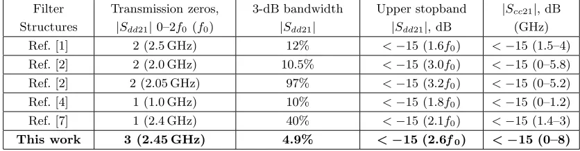
Table 1. Comparisons of measured results for some differential filters.
Filter Structures
Transmission zeros, |Sdd21|0–2f0 (f0)
3-dB bandwidth |Sdd21|
Upper stopband |Sdd21|, dB
|Scc21|, dB (GHz)
Ref. [1] 2 (2.5 GHz) 12% <−15 (1.6f0) <−15 (1.5–4)
Ref. [2] 2 (2.0 GHz) 10.5% <−15 (3.0f0) <−15 (0–5.8)
Ref. [2] 2 (2.05 GHz) 97% <−15 (3.2f0) <−15 (0–5.2)
Ref. [4] 1 (1.0 GHz) 10% <−15 (1.8f0) <−15 (0–1.2)
Ref. [7] 1 (2.4 GHz) 40% <−15 (2.1f0) <−15 (1.4–3)
This work 3 (2.45 GHz) 4.9% <−15 (2.6f0) <−15 (0–8)
3. MEASURED RESULTS AND DISCUSSION
Figure 5 shows the measured results of the proposed differential BPF. For the performances of DM in Figure 5(a), three transmission zeros are located at 1.62 GHz, 2.67 GHz and 5.06 GHz (3-dB bandwidth 4.9%, 2.36–2.48 GHz) respectively. The measured insertion loss is less than 2.4 dB while the return loss is over 13 dB in the passband. Furthermore, over 18-dB upper stopband is achieved from 2.54 to 6.45 GHz (2.6f0). For the performances of CM, as shown in Figure 5(b), over 15-dB stopband is obtained from 0
to 8.0 GHz (3.3f0). The slight frequency discrepancies between the measured and simulated results are
mainly caused by the limited fabrication precision and measurement errors.
For the purpose of comparison, Table 1 illustrates the measured results for some differential structures. Obviously, compared with former works, the upper stopbands for the differential mode and the stopbands for the common mode suppression of the proposed filter show better performances.
4. CONCLUSION
In this letter, a novel high selectivity differential BPF based on DBRs is proposed. The out-of-band suppression of DM and CM operation can be easily obtained by the bandstop transmission characteristic of the side-coupled coupled lines. Compared with former differential structures, the proposed differential filter has simpler circuit structures and wider common mode suppression. Good agreements between simulated and measured responses of the filter are demonstrated, indicating a good candidate for wireless applications.
ACKNOWLEDGMENT
This work is supported by the National Natural Science Foundation of China (6140010914), the 2012 Distinguished Young Scientist awarded by the National Natural Science Foundation Committee of China (61225001), Natural Science Foundation of Jiangsu Province (BK20140791) and the 2014 Zijin Intelligent Program of Nanjing University of Science and Technology.
REFERENCES
1. Shi, J., J.-X. Chen, and Q. Xue, “A novel differential bandpass filter based on double-sided parallel-strip line dual-mode resonator,”Microw. Opt. Technol. Lett., Vol. 5, 1733–1735, 2008.
2. Wu, C.-H., C.-H. Wang, and C. H. Chen, “Novel balanced coupled-line bandpass filters with
common-mode noise suppression,”IEEE Trans. Microw. Theory Tech., Vol. 55, 287–295, 2007.
3. Wu, C.-H., C.-H. Wang, and C. H. Chen, “Balanced coupled resonator bandpass filters using
multisection resonators for common-mode suppression and stopband extension,” IEEE Trans.
4. Horestani, A. K., M. Dur´an-Sindreu, J. Naqui, C. Fumeaux, and F. Mart´ın, “S-shaped complementary split ring resonators and their application to compact differential bandpass filters
with common-mode suppression,”IEEE Microw. Wireless Compon. Lett., Vol. 24, 149–151, 2014.
5. V´elez, P., J. Naqui, A. Fern´andez-Prieto, M. Dur´an-Sindreu, J. Bonache, J. Martel, F. Medina, and F. Mart´ın, “Differential bandpass filter with common-mode suppression based on open split
ring resonators and open complementary split ring resonators,” IEEE Microw. Wireless Compon.
Lett., Vol. 23, 22–24, 2013.
6. Feng, W. J. and W. Q. Che, “Novel wideband differential bandpass filters based on T-shaped
structure,” IEEE Trans. Microw. Theory Tech., Vol. 60, 1560–1568, 2012.
7. V´elez, P., M. Dur´an-Sindreu, J. Bonache, A. F. Prieto, J. Martel, F. Medina, and F. Mart´ın,
“Differential bandpass filters with common-mode suppression based on stepped impedance
resonators (SIRs),” Proc. IEEE MTT-S Int. Microw. Symp., 1–4, Seattle, WA, USA, Jun. 2013.
8. Su, T., S.-J. Wang, Y.-L. Zhang, and Z.-P. Li, “A compact DBR filter usingπ-network and dual-line equivalent circuit,”IEEE Microw. Wireless Compon. Lett., Vol. 23, 350–352, 2013.
9. Hua, C.-Z., C. Miao, and W. Wu, “A novel dual-band bandpass filter based on DBR,”Asia Pacific
Microwave Conference, 1383–1386, 2009.
10. Quendo, C., E. Rius, A. Manchec, Y. Clavet, B. Potelon, J.-F. Favennec, and C. Person, “Planar tri-band filter based on dual behavior resonator,” Proc. Eur. Microw. Conf., 269–272, Oct. 2005. 11. Srisathit, K., R. Phromloungsri, S. Patisang, and M. Chongcheawchamnan, “A new microstrip
duplexer using open circuited dual-behavior resonator,”Proc. Asia-Pacific Microw. Conf., Dec. 4– 7, 2005.
12. Manchec, A., et al., “Ku-band microstrip diplexer based on dual behavior resonator filter,” IEEE
MTT-S Int. Dig., 525–528, Long Beach, CA, Jun. 2005.
13. Eisenstant, W. R., B. Stengel, and B. M. Thompson,Microwave Differential Circuit Design using
Mixed-mode-parameters, Artech House, Boston, MA, 2006.
14. Deng, P. H. and J.-T. Tsai, “Design of microstrip cross-coupled bandpass filter with multiple
independent designable transmission zeros using branch-line resonators,” IEEE Microw. Wireless
Compon. Lett., Vol. 23, 249–251, 2013.
15. Hong, J. S. and M. J. Lancaster, Microstrip Filters for RF/Microwave Applications, Wiley, New