Design and Implementation of SOC VGA Controller
Using Spartan-3E FPGA
1
ARJUNA RAO UDATHA,
2B.SUDHAKARA RAO,
3SUDHAKAR.B.
1Dept of ECE, PG Scholar, 2 Dept of ECE, Associate Professor, 3Electronics, Scientist. 1Email: [email protected], 2Email: [email protected], 3Email: [email protected].
Abstract-This paper describes Design and Implementation of VGA (Video Graphics Array) controller using Verilog based in Spartan-3E Starter Board using Xilinx ISE 12.4 Tool and the VGA core IP (Intellectual Property) is designed to use with MicroBlaze Processor which is interfaced through On-chip Peripheral Bus (OPB) as on-chip peripheral using EDK 12.4 Tool. Field-programmable gate arrays (FPGAs) are especially suited to fulfill these requirements; FPGAs are very powerful, relatively inexpensive, and adaptable, since their configuration is specified in an abstract hardware description language. The main purpose of this project is to design and implement VGA Controller on FPGA. Therefore, the block diagram for VGA Controller is designed and the VGA Controller program is written based on the block diagram using Verilog HDL. Also, functions required for VGA Controller are included in the Verilog code and test bench is created to test the functions written to ensure the FPGA VGA Controller works correctly and accurately without errors. VGA Controller output signals generated directly by the FPGA chip and this is used to display images, graphics or textual data.
Index Terms - Spartan-3E Board, Block Diagram, Field-Programmable Gate Arrays (FPGAs), Verilog Hardware Description Language (Verilog HDL), VGA Controller.
1. INTRODUCTION
VGA (Video Graphics Array): Video Graphics Array the display standard for the PC. All PC display adapters support VGA and Windows machines boot up in “VGA mode before switching to higher resolutions. The term also often refers to the 15-pin plugs and sockets that connect the computer to the monitor. In this context, VGA refers to the traditional analog connection to a monitor in contrast to DVI, which is digital. Analog CRTs use VGA, and modern flat panel displays have both VGA and DVI inputs.
VGA resolution is 640x480 pixels with 16 or 256 colors. This base resolution is used when booting the PC and it is also used in Safe Mode for troubleshooting, because the display driver set at a higher resolution could be causing the problem. Although nothing stops a user from keeping this resolution, very little data would appear on screen (see illustration below). However, the small screens in handheld devices may well use VGA or even lower resolutions. VGA was introduced on IBM's PS/2 line in 1987 and quickly made the earlier CGA and EGA display interfaces obsolete, which were actually digital, but with lower resolution. In a short time, non-IBM vendors boosted the base resolution and colors to so-called "Super VGA." Over the years, resolution has been extended way beyond the original.
There are three signals -- Red, Green, and Blue -- that send color information to a VGA monitor. These three signals each drive an electron gun that emits electrons which paint one primary color at a point on the monitor screen. Signal levels between 0 (completely dark) and 0.7 V (maximum brightness) control the intensity of each color component, which combine to make the color of a dot (or pixel) on the monitor screen.
2. VGA CONTROLLER OPERATION
The horizontal sync generator outputs a single-cycle gate signal coincident with the leading edge of the horizontal sync pulse. This gate signal connects to the clock-enable of the vertical sync generator so it only updates its timing counter once per line of pixels. The gate signal of the vertical sync generator is used as an end-of-frame indicator to the external source of pixel data. It also resets the pixel buffer and clears its contents so the VGA generator starts from a completely cleared state on every frame.
The sync generators also output the horizontal and vertical blanking signals. These are logically-OR’ed to create a global blanking signal. The blanking signals are also combined with the lower order bits of the horizontal pixel counter to determine when to read more pixels from the buffer. For example, if the pixels are four bits wide, then a 16-bit word is needed from the buffer once every four clock cycles. So, the read operation is initiated whenever the video signal is not being blanked and the lower two bits of the pixel counter are both zero.
A full signal is sent to the external pixel data source to let it know when to stop filling the buffer. For a 255-entry FIFO, the full signal is raised when the upper five bits of the FIFO level signal are equal to 11111. This leaves seven empty slots in the FIFO to serve as a safety buffer for pixel data that the external source may already be generating in its own pipeline.
If the least-significant two bits of the counter are both zero, then the rd input to the pixel buffer will be driven high to initiate the reading of four more pixels, pN…pN+3. The buffer read operation begins at the rising edge of clock cycle N+1 and the 16-bits of pixel data are available on the buffer outputs at the rising edge of clock N+2. At this point, the new pixel data is loaded into the pixel register and the least-significant four bits containing pixel pN are sent to the color map circuitry. The color map circuit computes the RGB values, which are then latched at the beginning of cycle N+3. Simultaneously, pixel pN+1 is shifted into the lower four bits of the pixel register and the color map begins to compute the RGB values that will be output during cycle N+4.
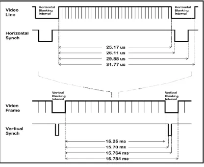
3. VGA SYNC SIGNALS TIMING
The timing for the VGA sync signals is shown in Figure 1. Negative pulses on the horizontal sync signal mark the start and end of a line and ensure that the monitor displays the pixels between the left and right edges of the visible screen area. The pixels are
sent on the red, green and blue signal lines within a 25.17 µs window. After this, a front porch interval of 0.94 µs is inserted before the horizontal sync signal pulses low for 3.77 µs.
After a back porch interval of 1.89 µs, the next line of pixels begins. Therefore, a single line of pixels occupies 25.17 µs of a 31.77 µs interval. The red, green and blue signals are blanked during the 6.6 µs interval comprised of the front porch, sync pulse and back porch. In an analogous fashion, negative pulses on the vertical sync signal mark the start and end of a frame made up of video lines and ensure that the monitor displays the lines between the top and bottom edges of the visible monitor screen. The lines are displayed within a 15.25 ms window. After this, a front porch interval of 0.45 ms is inserted before the vertical sync signal pulses low for 64 µs. After a back porch interval of 1.02 ms, the next frame begins. Therefore, a single frame of pixels occupies 15.25 ms of a 16.784 ms interval.
FIGURE 1. VGA SIGNAL TIMING
4. FIELD-PROGRAMMABLE GATE ARRAYS
reconfigurable FPGAs are generally favored in prototype building because the device does not need to be thrown away every time a change
This allows one piece of hardware to perform several different functions. Of course, those functions cannot be performed at the same time. Besides that, FPGAs are standard parts, they are not designed for any particular function but are programme
customer for a particular purpose.
FPGAs have compensating advantages, largely due to the fact that they are standard parts. There is no wait from completing the design to obtaining a working chip. The design can be programmed into the FPGA and tested immediately. Apart from that, FPGAs are excellent prototyping vehicles. When the FPGA is used in the final design, the jump from prototype to product is much smaller and easier to negotiate.
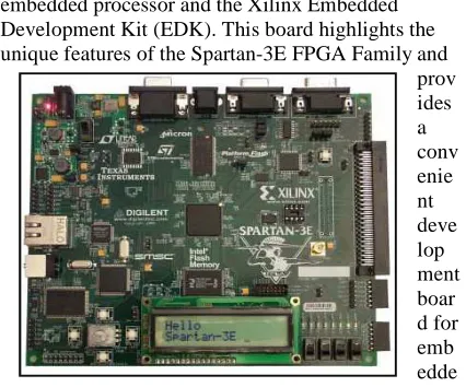
5. SPARTAN-3E STARTER KIT BOARD
The Spartan-3E Starter Kit board (Figure
demonstrates the basic capabilities of the MicroBlaze embedded processor and the Xilinx Embedded Development Kit (EDK). This board highlights the unique features of the Spartan-3E FPGA Family and
d processing Applications.
reconfigurable FPGAs are generally favored in prototype building because the device does not need to be thrown away every time a change is made. This allows one piece of hardware to perform several different functions. Of course, those functions cannot be performed at the same time. Besides that, FPGAs are standard parts, they are not designed for any particular function but are programmed by the
FPGAs have compensating advantages, largely due to the fact that they are standard parts. There is no wait from completing the design to obtaining a working can be programmed into the FPGA ested immediately. Apart from that, FPGAs are excellent prototyping vehicles. When the FPGA is used in the final design, the jump from prototype to product is much smaller and easier to negotiate.
3E STARTER KIT BOARD
(Figure 2)
demonstrates the basic capabilities of the MicroBlaze embedded processor and the Xilinx Embedded
This board highlights the
6. ADDING CUSTOM HARDWARE IPS FOR SYSTEMS
Step 1:
Create the Custom IP and open the vga_cntrl.v, user_logic.vhd and add necessary
logic in vga_cntrl.v and user_logic.vhd files.
Step 2:
Using the IP Catalog from
the project, make bus connections, generate address for the vga_cntrl instance, add necessary ports to the
instance, name them appropriately and bring out the data port and add ports to FPGA pins in the UCF file.
In the IP Catalog tab, expand Project Local pcores and add the custom peripheral
hardware system. Select the
lock down the addresses of all peripherals except for vga_cntrl_0 and generate
Step 3:
Develop simple software application, generate and download the bit-stream. Verify that the design operation. As shown in figure
FIGURE 3.ADDING CUSTOM HARDWARE IPS FOR SYSTEMS
7. VGA CONTROLLER PARAMETERS AND I/O
The following generic parameters affect the operation of the VGA generator:
FREQ: This parameter sets the master operating frequency of the controller (in units of MHz). This frequency is used to calculate the time delays for the horizontal and vertical sync pulses. The default value for the SPARTAN-3E STARTER Board is 50 MHz. CLK_DIV: Setting this parameter to a value greater user_logic.vhd and add necessary declarations and logic in vga_cntrl.v and user_logic.vhd files.
from XPS, add vga_cntrl to the project, make bus connections, generate address instance, add necessary ports to the
appropriately and bring out the data port and add ports to FPGA pins in the UCF file.
tab, expand Project Local pcores and add the custom peripheral vga_cntrl to the hardware system. Select the Addresses filter and lock down the addresses of all peripherals except for
generate the address.
Develop simple software application, generate and stream. Verify that the design
The following generic parameters affect the operation
from the buffer and delivered to the monitor. For example, if FREQ=50_000 and CLK_DIV=2, then pixels are sent to the monitor at a rate of 25,000,000 per second. PIXEL_WIDTH: This parameter gives the bit-width of a pixel. Allowable values are 1, 2, 4, 8 and 16. PIXELS_PER_LINE: This parameter determines the number of pixels displayed in the active portion of each video scan-line. LINES_PER_FRAME: This parameter sets the number of lines of pixels displayed in the active portion of each video frame.
NUM_RGB_BITS: This is the number of bits of color information in each of the red, green and blue components. Set this to 1 for the SPARTAN-3E Board. FIT_TO_SCREEN :If this Boolean parameter is set to true, then the sync generators are configured so that the given number of pixels and lines fill the entire width and height of the screen, respectively. Setting this parameter to false, however, embeds the active video region into a standard 31 KHz/ 60 Hz horizontal / vertical video frame.
8. VGA DISPLAY PORT
The Spartan-3E Starter Kit includes a VGA display port via a DB15 connector. Connect this port directly to most PC monitors or flat-panel LCDs using a standard monitor cable.
3-Bit Display Color Codes:
The Spartan-3E FPGA directly drives the five VGA signals via resistors. Each color line has a series resistor, with one bit each for VGA_RED, VGA_GREEN, and VGA_BLUE. The series resistor, in combination with the 75ohm termination built into the VGA cable, ensures that the color signals remain in the VGA-specified 0V to 0.7V range. The VGA_HSYNC and VGA_VSYNC signals using LVTTL or LVCMOS33 I/O standard drive levels. Drive the VGA_RED, VGA_GREEN, and VGA_BLUE signals High or Low to generate the eight colors shown in Figure 4.
FIGURE 4.VGA CONNECTIONS FROM SPARTAN 3E
9. VERILOG HARDWARE DESCRIPTION LANGUAGE
Verilog HDL is a description language that can be used to model a digital system at many levels of abstraction ranging from the algorithmic-level to the switch-level. The complexity of the digital system being modeled could vary from that of a simple gate to a complete electronic digital system, or anything in between. The digital system can be described hierarchically and timing can be explicitly modeled within the same description.
The Verilog HDL language includes capabilities to describe the behavioral nature of a design, the dataflow nature of a design, a design’s structural composition, delays and a waveform generation mechanism including aspects of response monitoring and verification, all modeled using one single language. In addition, the language provides a programming language interface through which the internals of a design can be accessed during simulation including the control of a simulation run.
The language not only defines the syntax but also defines very clear simulation semantics for each language construct. Therefore, models written in this language can be verified using a Verilog simulation. The language inherits many of its operator symbols and constructs from the C programming language. Verilog HDL provides an extensive range of modeling capabilities, some of which are quite difficult to comprehend initially. However, a core subset of the language is quite easy to learn and use. This is sufficient to model most application. The complete language, however, has sufficient capabilities to capture the descriptions from the most complex chips to a complete electronic system.
10. PRINCIPLES OF VGA
(three-bit) digital-to-analog converter (DAC).The four (eight) possible levels on each analog input are combined by the monitor to create a pixel with one of 4 x 4 x 4 = 64 (8 x 8 x 8 = 512) different colors. So the six (nine) digital control lines let us select from a palette of 64 (256) colors.
11. VGA CONTROLLER ALGORITHM
Module 2: The outputs for the horizontal and vertical sync pulses are declared. These outputs are registered to make sure they are not affected by combinational logic delays in the VGA generator circuitry.
Module 3: These lines declare the outputs for driving the address lines of the RAM and the inputs for vertical position of the line on the screen are declared on these lines. We will call these the horizontal or pixel counter, and the vertical or line counter, respectively. The line period is 31.77 µ
clock cycles, so the pixel counter needs at least nine bits of resolution. Each frame is composed of 528 and its registered counterpart that is used in the next pipeline stage.
Module 5: The pixel and line counters are set to zero when the reset input is high. The reset is only activated at the start of the operation of the VGA generator circuitry and is not used during the normal operations. The pixel counter is incremented on the rising edge of the 50 MHz pixel clock. The vertical line counter is clocked by the rising edge of the horizontal blanking pulse, so it increments only after a line of pixels is completed.
The registered horizontal sync output is updated on every pixel clock. The registered vertical sync output is updated whenever a line of video is completed. The values that are placed in these registers at specific times are determined in the statements which follow.
analog converter (DAC).The four (eight) possible levels on each analog input are combined by the monitor to create a pixel with one of = 512) different colors. So the six (nine) digital control lines let us select from a
VGA CONTROLLER ALGORITHM
VGA Controller Algorithm is divided into five modules:
Module 1: By taking the 50 MHz clock frequency of the SPARTAN-3E STARTER Board, generates 108.333 MHz frequency required for pixel clock. This clock sets the maximum rate at which pixels can be sent to the monitor.
horizontal and vertical sync pulses are declared. These outputs are registered to make sure they are not affected by combinational logic delays in the VGA generator circuitry.
These lines declare the outputs for driving RAM and the inputs for receiving the data from the RAM. These are the declarations for the outputs which drive the control
The counters that store the current horizontal position within a line of pixels and the vertical position of the line on the screen are declared on these lines. We will call these the horizontal or pixel counter, and the vertical or line counter, ely. The line period is 31.77 µs which is 381 clock cycles, so the pixel counter needs at least nine bits of resolution. Each frame is composed of 528 and its registered counterpart that is used in the next
line counters are set to zero when the reset input is high. The reset is only activated at the start of the operation of the VGA generator circuitry and is not used during the normal operations. The pixel counter is incremented on the MHz pixel clock. The vertical line counter is clocked by the rising edge of the horizontal blanking pulse, so it increments only after
The registered horizontal sync output is updated on vertical sync output is updated whenever a line of video is completed. The values that are placed in these registers at specific times are determined in the statements which
This line sets the range for the horizontal pixel counter to be [0,380]. When the counter reaches 380, it rolls over to 0. Thus, the counter has a period of 381 pixel clocks. With a pixel clock of 12 MHz, this translates to a period of 31.75
determines the active and inactive intervals of the registered horizontal sync output. The sync signal goes low on the cycle after the pixel counter reaches 291 and continues until the cycle after the counter reaches 337. This gives a low horizontal sync pulse of (337-291)=46 pixel clocks. With a pixel clock of 50 MHz, this translates to a low
sync pulse of 3.83 µs. The sync pulse starts 292 clocks after the line of pixels begins, which translates to 24.33 µs. This is less than the 26.11
before. The difference of 1.78 ms translates to 21 pixel clocks. This time interval corresponds to the 23 blank pixels that are placed prior to the 256 viewable pixels (minus two clock cycles for pipelining delays).
12. DESIGN AND I
Install the Xilinx ISE software
to update the software version included with your kit. Install the Unified Logic Development Platform software. Plug in the Spartan
using the power supply included with the kit. Attach the board to the host PC using the supplied USB
cable.Attach an RS-232 cable from connector J36 on the Spartan-3E Starter Kit Board to your host PC machine. If your PC does not have a serial port, you VGA Controller Algorithm is divided into five
By taking the 50 MHz clock frequency of 3E STARTER Board, generates 108.333 MHz frequency required for pixel clock. This clock sets the maximum rate at which pixels can
This line sets the range for the horizontal pixel When the counter reaches 380, it rolls over to 0. Thus, the counter has a period of 381 pixel clocks. With a pixel clock of 12 MHz, this translates to a period of 31.75 µs. This line determines the active and inactive intervals of the l sync output. The sync signal goes low on the cycle after the pixel counter reaches 291 and continues until the cycle after the counter reaches 337. This gives a low horizontal sync pulse 291)=46 pixel clocks. With a pixel clock of anslates to a low-going horizontal µs. The sync pulse starts 292 clocks after the line of pixels begins, which translates s. This is less than the 26.11 µs we stated before. The difference of 1.78 ms translates to 21 ks. This time interval corresponds to the 23 blank pixels that are placed prior to the 256 viewable pixels (minus two clock cycles for pipelining delays).
IMPLEMENTATION
nx ISE software. It may be necessary software version included with your kit. Install the Unified Logic Development Platform software. Plug in the Spartan-3E Starter Kit Board using the power supply included with the kit. Attach the board to the host PC using the supplied USB
can use an Serial-to-USB adapter. As shown in Figure 5.
If your Serial-to-USB adapter has hex heads on each
side of the D-shell connector, you may need to remove the heads from either the adapter or the connector on the evaluation board. Power up the Spartan-3E Starter Kit Board. Powering the board up with the USB cable connected may cause Windows to look for a driver. Under Windows XP a wizard appears to which you should NOT request Windows to look over the Internet (say no to the first screen) and then accept the default of automatically searching locally (second screen). Run the Unified Logic IDE by double-clicking its icon on the Windows desktop or by selecting it from the Start menu. Results as shown in Figure 6.
FIGURE 5. BLOCK DIAGRAM OF VGA CONTROLLER.
FIGURE 6. RESULTS
13. CONCLUSION
In conclusion, VGA Controller could be constructed easily without constructing the circuit manually; just to write a behavioral model or few behavioral models based on its logic flows, then simulate it with test benches, synthesize it with netlist, and finally program it onto FPGA. It is very effective as this VGA Controller only needs new data to change to other design display. Thus, FPGA-based VGA controller might be a good choice as it is easy to be designed and tiny to be used.
REFERENCES
[1] Embedded Systems Tools Reference Manual:
http://www.xilinx.com/ise/embedded/est_rm.pdf [2] Embedded System Tools Guide:
www.xilinx.com/ise/embedded/est_guide.pdf [3] Processor IP Reference Guide:
www.xilinx.co.jp/ise/embedded/proc_ip_ref_gui de.pdf