310-103000-000 Price: $7.00
MODCOMP III COMPUTER
REFERENCE MANUAL
May 1972
Modular Computer Systems 1650 West McNab Road
I.
II.
CONTENTS
MODCOMP III CHARACTERISTICS GENERAL CHARACTERISTICS
Memory System
General Register File Arithmetic Module
Read-Only Memory Controller Input/Output System
Interrupt System Control Panel
Physical Characteristics MODCOMP SOFTWARE
Executive Systems Language Processors
Diagnostics, Utilities, Math Library MODCOMP DATA PROCESSING PERIPHERALS
MEASUREMENT, CONTROL AND COMMUNICATION EQUIPMENT High Level Analog Input Subsystem
Wide Range Solid State Analog Input Subsystem Wide Range Relay Analog Input Subsystem
Input/Output Interface Subsystem Communications Multiplexers Communications Channels SYSTEM EXPANOARIT.ITY
MULTIPROCESSOR CONFIGURATIONS CENTRAL PROCESSOR DESCRIPTION
INFORMATION FORMATS Basic Formats
Arithmetic Data Formats Character Formats REGISTER FILE
ADDRESSING
Memory Word Addressing Byte Addressing
Bit Addressing
DEDICATED MEMORY LOCATIONS SECOND MEMORY PORT
READ-ONLY MEMORY CONTROLLER OPERATIONAL INTEGRITY FEATURES
Memory Parity
Unimplemented and Call Instructions Undefined Instructions·
Floating Point O~erf1ow
Doub1eword Operand Register Storage Power Fail Safe/Auto Start
System Protect Feature REAL-TIME CLOCK
III. INSTRUCTION SET OVERVIEW
LOAD, STORE AND TRANSFER INSTRUCTIONS LDM LDI LOS LOX STM STI STS STX LBX
Effective Byte Address Generation SBX LFM LFS LFX SFM SFS SFX TRR TRRB
3-16
SUR 3-16
SURB 3-16
MPM 3-17
MPS 3-17
MPX 3-17
MPR 3-18
DVM 3-18
DVS 3-18
DVX 3-19
DVR 3-19
CRMB 3-19
CRSB 3-20
CRXB 3-20
TRO 3-20
TTR 3-21
TTRB 3-21
LO,;ICAL INSTRUCTIONS 3-22
ETM 3-22
ETI 3-22
ETS 3-22
ETX 3-23
ETMM 3-23
ETMB 3-23
ETSM 3-24
ETSB 3-24
ETXM 3-24
ETXB 3-25
ETR 3-25
ETRB 3-25
ORM 3-26
ORI 3-26
ORS 3-26
ORX 3-26
ORMM 3-27
ORSM 3-27
ORXM 3-27
ORR 3-27
ORRB 3-28
XOM 3-28
XOI 3-28
XOS 3-29
XOX 3-29
XOR 3-29
XORB 3-29
TOR 3-30
3-30
TRXB 3-31
TERB 3-31
FLOATING POINT INSTRUCTIONS 3-32
Introduction 3-32
Data Formats 3-32
FLOATING POINT INSTRUCTION MNEMONICS 3-33
GENERAL RULES 3-33
Overflow 3-34
FAR 3-34
FSR 3-34
FMR 3-34
FDR 3-34
FARO 3-36
FSRD 3-36
FMRD 3-37
FDRD 3-37
FAM 3-37
FSM 3-38
FMM 3-38
FDM 3-39
FAMD 3-39
FSMD 3-39
FMMD 3-40
FDMD 3-40
SHIFT INSTRUCTIONS 3-41
LAD 3-41
RAD 3-41
LAS 3-42
RAS 3-42
LLD 3-42
RLD 3-42
LLS 3-43
RLS 3-43
LRS 3-43
BIT MANIPULATION INSTRUCTIONS 3-44
LBR 3-44
LBRB 3-44
ABMM 3-45
ABMB 3-45
ABSM 3-45
ABSB 3-46
ABXM 3-46
ABXB 3-46
ABR 3-47
ABRB 3-47
ZBMM ZBMB ZBSM ZBSB ZBXM ZBXB ZBR ZBRB OBMM OBSM OBXM OBR OBRB XBR XBRB TBMB TBSB TBXB TBRB CBMB CBSB CBXB GMR GMRB
BYTE MANIPULATION INSTRUCTIONS MUR
MLR MBR MBL IBR
UNCONDITIONAL BRANCH INSTRUCTIONS BLM
BLI BRU HOP BRX
CONTROL INSTRUCTIONS HLT
NOP SPR
RIA REX RMI CAR CIR
INPUT/OUTPUT INSTRUCTIONS ISA ISB ISC ISD IDA IDB IDC IDD OCA OCB OCC OCD ODA ODB ODC ODD IV. PRIORITY INTERRUPTS
OVERVIEW
LEVEL ASSIGNMENTS
INTERRUPT OPERATION AND PROGRAM CONTROL
INTERRUPT SUB-LEVEL OPERATION AND PROGRAM CONTROL TRAPS
Unimplemented Instruction Trap Memory Parity Trap
System Protect FLOATING POINT OVERFLOW
POWER FAIL SAFE/AUTO START INTERRUPT V. INPUT/OUTPUT
OVERVIEW
INSTRUCTION EXECUTION SEQUENCE TRANSFER FORMATS 0
REGISTER I/O TRANSFER MODES INPUT/OUTPUT INTERRUPTS DIRECT MEMORY PROCESSOR Transfer Initiation Data Chaining
Register File
PERIPHERAL DEVICE ASSIGNMENTS PROGRAMMING CONSIDERATIONS
REGISTER I/O INTERRUPT MODE SEQUENCE New command Initiation
Response to Service Interrupt REGISTER I/O TEST AND TRANSFER MODE DIRECT MEMORY PROCESSOR I/O MODE
New' Conunand Initiation Response to Data Interrupt Response to Service Interrupt OUTPUT COMMAND FORMATS
Select Format Control Format No Op Conunand
Interrupt Disconnection and Termination Transfer Initiate
INPUT STATUS FORMAT VI. OPERATOR CO~TROLS
INDICATORS Data
Parity Error Run
Power On SWITCHES
Data Entry Panel Lock Master Clear Fill
Run/Halt Single Cycle Enter
Step P
Console Interrupt Display
Enter R
Register Select CONTROL PANEL OPERATION
Display Register Load Register
FILL
Load Memory Display Memory Start Program
Single Cycle Program
1-1 5-1
2-1 3-1 3-2 4-1 4-2 5-1 6-1
A
B
C
D E
F
G
MODCOMP III Block Diagram
INPUT/OUTPUT SUBS~STEM BLOCK DIAGRAM
Dedicated Memory Locations Symbols and Abbreviations
TABLES
Floating Point Register Selections INTERRUPT LEVEL ASSIGNMENTS
Sub-Level Assignments
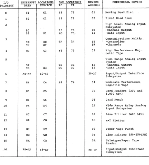
Peripheral Device Interrupt Assignments REGISTER DATA
APPENDICES
Hexadecimal to Decimal Conversion Character Codes
Peripheral Device Commands and Tests Divide
Instruction List
Table of Powers of Two and Sixteen Floating Point Number Examples
1- 2 5- 2
2- 8 3- 3 3-33 4- 2 4- 4 5- 7 6- 3
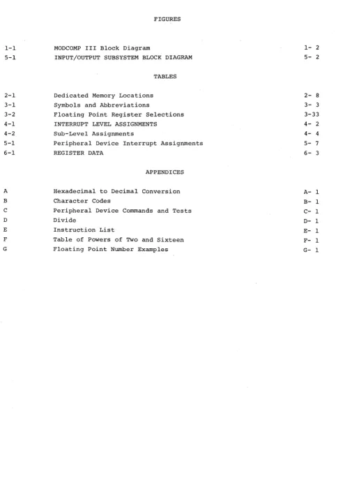
[image:13.613.57.552.37.748.2]I. MODCOMP III CHARAClERISllCS
MODCOMP III is an BOO-nanosecond, l6-bit computer having many of the characteristics of 32-bit computers. It is designed with unique processing capabilities and with the capacity to be gracefully upgraded with new features and performance abilities as computer and component technologies advance.
MODCOMP III consists of a set of functional modules implemented with the present state of the art in MSI, IC, and core memory technology and designed to be upgraded with LSI and other advanced technologies when available. All data transfers and manipulations within the computer are controlled by a highly-flexible read-only memory (ROM) controller. The ROM controller provides a rich instruction set
including bit, byte, word, doubleword, tripleword (including floating point) and file manipulation instructions. It also provides an open-ended design which enables user firmware and new macro instructions to be added to the computer.
MODCOMP III is available in several configurations starting with the basic model 111/5. The descriptions in this text apply to both the MODCOMP 111/5 and III/IS unless other-wise noted. The only differences between MODCOMP 111/5 and III/IS are the optional Direct Memory Access Channels and Second Memory Port which are not available on the 111/5. Configurations with increasing processing capabilities are available from a single MODCOMP III computer having up to 64K words of directly addressable memory to a multi-processor configuration having up to l20K words of memory. The broad
range of configurations available means that there is a MODCOMP III system ideally suited for any of a wide spectrum of real-time applications including measurement, control and communications. And this spectrum is extended on the lower side by com-patible members of the MODCOMP family - the 16 bit MODCOMP II in the middle and the 16 bit mini, MODCOMP I, at the lower end.
GENERAL CHARACTERISTICS
The organization of MODCOMP III is shown in Figure 1-1. The components which comprise the MODCOMP 111/5 are shown within the dashed lines. Other systems consist of the basic component set plus different combinations of the components shown outside of the dashed lines.
4K WORDS (64 ~
4K WORDS (60) 4K WORDS '(56)
POINT INSTRiJCTIONS
MULTIPLY/ DIVIDE INSTRUCTIONS
4K WORDS (16)
I - - - - -,
4K WORDS (12)
I
I
!K
~R~
~)
W
CONTROLI
.4K WORDS PANEL L
• CORE
I
MEMORYSECOND
I
SYSTEM WITH1\
<==>!
BYTE PARITY ~j<;
MEMORY
!
PORT :,., _ _ _ _ . . .
I GENERAL
I
REGISTER~
I
FILEV
...,
15 GEN. REGS. F"--....---.././I
I ' f v•
I
II/O BUS IIINPUT/OUTPUT SYSTEM
~
WITH TTYI
AND PTR CONTROLLERI \ ;
MODULAR BUS
256 CUSTOM(1,024) 256 CUSTOM
128 CUSTOM I/O 128 DMP
1 - - - 1 - - - 1 - - ,
128 BASIC
I
')
v
128
INSTRUCTION
I
SET READ-ONLY MEMORY CONTROLLER ARITHMETIC MODULE INTERRUPT SYSTEM WITH POWER FAIL SAFE/AUTOSTART
I
I
I
I
. I
I
I
I
t
I
I
I
I
LI1
I
~-
r---
_ -I-. I- _.!..
L~L~ _ • I-..J.... ___ I
r---1
A;:;.K--'~
I
SYSTEML
I PROTECT'-I- - -, - - - ~ FEATURE
4 LEVELS ( 8) 4 LEVELS (12) 4 LEVELS (16) DIRECT
MEMORY PROCESSOF I -16 CHANS.
DIRECT MEMORY CHANNELS I
-(1-4)
EXECUTIVE I--FEATURES
4 LEVELS (20) 4 LEVELS (24)
-r
625 CPSJ
I-.._....jl
PT READER....
-4 LEVELS (28) 4 LEVELS (32)
Figure 1-1 MODCOMP III Block Diagram
[image:15.613.70.566.56.677.2]Memory System
• 4,096 to 65,536 l6-bit words, expandable by 4K word modules • 400 nanosecond access time
800 nanosecond full cycle time
Parity bit per byte standard in all models (even parity)
• All memory locations directly addressable
Seven memory addressing modes provided including indirect, indexed and immediate • Dual, concurrent access available in multiprocessor configurations
Memory protect option
General Register File
• 15 addressable, 16 bit, general purpose registers
• 7 of the general registers us.able as index registers • All 15 registers usable for short indexing operations
• 800 nanoseconds execution time for typical register-to-register instructions
Arithmetic Module
Parallel operation
Full set of arithmetic, logical, compare, and shift capabilities Execution times
Add, Subtract, And, Or, Exclusive Or (Reg. -to-Reg.) Add, Subtract, And, Or, Exclusive Or (Mem.-to-Reg. ) Multiply (Reg. -to-Reg.) = 6.0 u sec., (Mem.-to-Reg.) Divide (Reg. by Reg.) =11.0 u sec.,
Implemented with four MSI modules
Read-Only Memory Controller
200 nanosecond cycle time 40-bit word length
(Mem. by Reg.)
256 words in basic computer, expandable to 1,024
0.8 u sec. 1.6 u sec. 7.2 u sec. 12.2 u sec.
optional instructions including floating point arithmetic and fixed point multiply/divide
User firmware can be added
Input/Output System
Program controlled transfers to/from 63 peripheral devices Transfers synchronized by interrupts
Transfers can be made from any general register to any device
Transfers are made over a differentially buffered input/output bus which isolates the computer from external cable and controller delays
Direct Memory Processor available for automatic block transfers to/from 16 peripheral devices on a multiplexed basis
Direct Memory available for transfers at rates up to 1.25M words/sec.
Four standard levels-two input/output, Power Fail Safe/Auto Start, and Un-implemented Instruction trap
Interrupts expandable in groups of four levels to a total of 32 levels. In addition, each of the two priority levels (OC,OD) are connected to 17 unique psuedo-priority levels which can be connected to up to 128 sublevels, each with a unique (dedicated) memory pointer •
• Complete program control of the Request, Enable*, and Active states of each level System Protect Feature includes memory protect and privileged instruction trap capabilities which enable the computer to operate in either a protected or an unprotected mode
• Executive features include a real-time clock (120 Hz), console interrupt, task scheduler interrupt, and one external interrupt
Control Panel
Capability to display or modify the contents of any memory location, general register or most non-programmable registers
Program fill switch Control panel lock switch
Master Clear to clear computer and peripherals
Optional Console Interrupt executive feature causing an interrupt request to Level E
Physical Characteristics
0-55°C operating ambient temperature range 120
:!:.
10% vac, 50:!:.
2 Hz or 60±
2 HzPackaged for mounting in a standard 19-inch wide cabinet. Occupies 26 inches vertically
Standard package will hold 32K words of memory and all computer options
MODCOMP SOFTWARE
Executive Systems
Three ~odular ~pplication E~ecutive (MAX) systems are available with MODCOMP III computers to meet the requirements of a wide range of machine operating environments.
MAX I is a core resident operating system which improves machine utilization efficiency in assembling, debugging and related operations.
MAX II is a disc operating system which accepts a batch job input consisting of
assemblies, compilations and/or executions. A core resident version is also available for non-disc systems.
~
!!!
is a real-time multiprogramming executive which provides complete task scheduling, initiation, termination and I/O services. This system will control the execution of any mixture of foreground/middleground and background tasks. Unpro-tected (middleground) tasks can be brought on-line without disturbing other proUnpro-tected(foreground) tasks. Batch processing can be performed in the background. A
core-only version is available for dedicated applications.
Language Processors
Several language processors are available with MODCOMP systems.
FORTRAN IV - The MODCOMP FORTRAN compiler meets the full ANSI FORTRAN specifications. It is designed to produce efficient code by using all machine capabilities such as all registers in the register file and all instructions. It produces assembly language output, permitting the programmer to optimize further. The programmer can also write programs in any desired mixture of compiler and assembly languages. Avail-able in a core-resident or overlay version under MAX II and MAX III.
Extended Fortran IV - This FORTRAN compiler is an extension of FORTRAN IV as defined above containing random access I/O operations through DEFINE FILE. This compiler contains block level optimi~ation to produce efficient object code. Available in core resident or overlay versions under MAX II or MAX III.
BASIC - This multi-user system is a subset of the Dartmouth BASIC system operating under either MAX II or MAX III. It enables users having no previous programming experience to write programs in a simple, quickly learned language.
Macro Assembler - This big machine class assembler has an extensive set of .directives and error diagnostics as well as a macro processor. It accepts conditional assembly statements, assembly time branches and macro exits. It is a two-pass assembler, operating under MAX II and MAX III. Available in core-resident or overlay versions.
Assembler - The assembler is a subset of the macro assembler. It generates reloca-table as well as absolute object code and operates under MAX I, II or III.
FORTRAN Coded Assembler - The assembler is available in FORTRAN source language. This assembler operates on the IBM 360/370 and is compatible with the MODCOMP III assembler in both syntax and binary output. The user can therefore assemble programs on the IBM 360/370 and then run them on the MODCOMP III with no modifications. Operates under OS or DOS in 65K bytes.
Diagnostics, Utilities, Math Library
MODCOMP DATA PROCESSING PERIPHERALS
Modular peripherals are available for a broad spectrum of applications including pro-gram preparation, data processing and system support functions. All peripherals are supported by the appropriate MAX system. The basic specifications for each device are summarized below.
Page Printers Paper Tape Reader
- ASR-33, ASR-35, KSR-35 Teletypes - 625 characters per second
Paper Tape Reader and Punch - 625 characters per second read, 110 characters per Card Readers
Card Punch
second punch
- 300-1000 cards per minute - 100 cards per minute High Speed Serial Printer
Line Printers
- 50-150 lines per minute, 132 columns - 600 lines per minute, 80-132 columns Magnetic Tape Units
Fixed-Head Discs
Moving-Head Discs
- 12.5/45 IPS, 7/9 track, 556/800 BPI, industry compatible NRZ. 45 IPS, 9 track, 1600 BPI industry compatible Phase Encoded.
- 8.5/17/25 millisecond average access time Capacity range - 65K to 1M words
Transfer rates - 68K-247K words per second - 20 millisecond average latency
Capacity range - over 1.2M, 13M and 26M words. Transfer rates - 97.8K words and l56K words per second
MEASUREMENT, CONTROL AND COMMUNICATION EQUIPMENT
A complete range of analog input, analog output, digital input, digital output and communication equipment is available to operate with MODCOMP computer systems. This equipment has all been designed together expressly to operate with MODCOMP systems. Therefore hardware formats, interfaces, cabling and power supplies are the same in all units to facilitate customer usage and minimize spares requirements.
High Level Analog Input Subsystem
Channel Capacity - 16-128 Channels single-ended or 8-128 Channels differential Input Range -±10.24 volts full scale or +102.4 volts full scale
Throughput Rate - 50,000 Channels per second max. Overall Accuracy - +0.05% Full Scale ~1/2 LSB
Wide Range Solid ~ Analog Input Subsystem Channel Capacity
Input Ranges Throughput Rate Overall AcCuracy Auto Ranging Zero Suppression
- 8-128 Channels
- 12 Programmable ranges from ~5 MV to +10.24V Full Scale - 20,000 Channels per second max.
- +0.05% Full Scale ~1/2 LSB
Channel Capacity Input Ranges Throughput Rate Overall Accuracy Auto Ranging
Zero Suppression
- 8-512 Channels
- 12 Programmable ranges from ~5 MV to +10.24V Full Scale - 200 Channels per second max.
- +10 Microvolts or +0.05% Full Scale - Standard
- Optional
Input/Output Interface Subsystem Channel Capacity
Digital Inputs Digital Outputs Analog Outputs
Serial Communica-tions Interface Interval Timer I/O Interrupts External Inter-rupts
Synchronizer
- 16 Input/Output channels of 16 bits each plus expander chassis (up to 2048, 16 bit channels)
- Micrologic, positive voltage, negative voltage, bipolar voltage, contact sense. (Isolated and filtered inputs) - Micrologic, positive voltage, negative voltage, electronic
switch, contact closure, pulse output, and AC output (TRIAC) - 12 Bits binary, including sign
- ~10 volts, ~20 volts, 1 to 5 rna, 4 to 20 rna, 10 to 50 rna - RS 232 or 20 rna current loop (TTY compatible)
- Provides programmable timing interrupt or 'watchdog' timer - Provides 8 data interrupts and/or 8 service interrupts - Provides signal conditioning and driver for 16 external
interrupts provided the Executive Feature for External Interrupt is included in the system
- Provides 'handshake' data transfer
Communications Multiplexers Types
Channel Capacity
- Universal, operates in synchronous and/or asynchronous mode. Asynchronous, operates in asynchronous mode only.
Universal, 4 to32 full duplex channels expandable in groups of 4 up to 64 full duplex channels.
Asynchronous, 2 to 32 full duplex channels expandable in groups of 2 up to 128 full duplex channels.
Communications Channels
Clocking Mode Communication Interfaces Baud Rate Codes Stop bits Parity Echo
ASYNCHRONOUS - Asynchronous
- EIA RS-232-C Modems, TTl Modems, TTy 60/20 ma Current loop - Patchable from 75 to 9600 baud with a maximum of five different
baud rates per multiplexer (to 50KB.on request) - Program selectable - 5, 6, 7, or 8 bits plus parity - Program selectable - 1 or 2
- Program selectable - none, odd, even
Communications Channels (Cont'd)
Clocking Mode Communications
Interfaces Baud Rate
Code Parity
Synch Character
SYNCHRONOUS
- Synchronous
- EIA RS-232-C Modems, TTL Modems
Patchable to 5DK baud with a maximum of five different baud rates per multiplexer
- Program selectable - 5, 6, 7, or 8 bits plus parity - Program selectable - none, odd, even
SYSTEM EXPANDABILITY
The modular design makes the MODCOMP III computer easily expandable. The basic assembly is capable of containing all system features. Core memory up to a total of 64K words can be added by plug-in insertion of additional 4K memory modules. The ROM and interrupts are also modular and are field expandable. Even the concurrent memory access path (second port)*can be added in the field. Therefore, a MODCOMP SYSTEM can always be upgraded from one model to the next higher model. It can
even be converted into a multiprocessor system if the need for a substantial increase in computing capability arises.
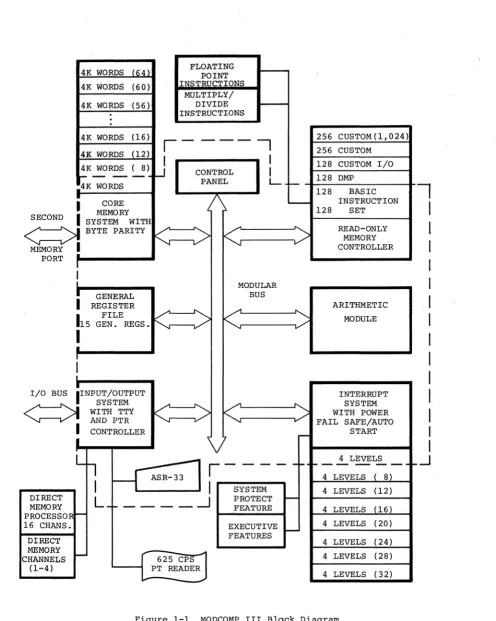
MULTIPROCESSO_R CONFIGUR,ATIONS
The MODCOMP III/70 is a multiprocessor having two CPU's and both private and shared memory modules. The range of multiprocessor configurations available is shown in Figure 1-2.
Each of the two computer cabinets can contain from 4K to 64K words of memory, and each CPU can address up to 64K words. Memory can be connected to the CPU in the other cabinet on an SK word basis, except for the highest memory section which can be 4K
as well as SK.
The lower SK memory section cannot be shared because the lower 4K module in each computer is required for the dedicated memory locations. The 4K module having addresses 4-SK could be omitted, but this would leave a memory address gap.
The private memory in each CPU must be large enough to contain the individual MAX III operating systems. The shared memory is used for a data communication area through global common.
The CPU-to-CPU communication interrupt is generated by execution of the Request Multiprocessor Interrupt instruction. Whenever this instruction is executed in one CPU, an interrupt signal is sent to Level 3 in the other CPU.
I
I
I
CPU 1 SK
•
•
•
SK1
COMMUNICATION SKINTERRUPT SK
•
• •
or4K
CPU 2 SK
•
• •
SK [image:22.613.135.549.554.694.2]II. CENTRAL PROCESSOR DESCRIPTION
INFORMATION FORMATS
Basic Formats
The l6-bit word is the basic information format of the MODCOMP I I I computer. The bit designations in the computer word are:
WORD FORMAT
WORD
o
1 2 3 4 5 6 7 8 9 10 11 12 13 14 15Some instructions operate on doublewords which consist of 32 bits of data stored in two consecutive register or memory locations.
EVEN REGISTER
ODD REGISTER
o
o
DOUBLEWORD FORMAT
MORE SIGNIFICANT WORD
15
LESS SIGNIFICANT WORD
15
To be an operand for a doubleword instruction which operates on register contents, the more significant word must be stored in a register location having an even address and the less significant word must be stored in the next higher (odd) register.
Many instruction and peripheral devices operate on eight-bit bytes which are packed two per register or memory location in the format:
BYTE DESIGNATIONS
BYTE 0 BYTE 1
o
7 8 15Hexadecimal (base 16) digits are often used as a convenient means of representing binary byte, word or double word values. The hexadecimal word format is:
valent decimal numbers are listed in Appendix A. In the text, hexadecimal numbers appear in the form N16 .
Arithmetic Data Formats
Fixed Point Binary Integer Format - This is the standard arithmetic data format in the MODCOMP III and consists of a sign bit and 15 or 31 data bits. The most significant bi t is the sign bit, which i's defined:
Sign Sign
0, Positive or Zero Quantity 1, Negative Quantity
Two's complement representation is used for negative numbers. The principal fixed point arithmetic formats are:
SINGLE PRECISION FIXED POINT DATA FORMAT
o
1 15DOUBLE PRECISION FIXED POINT DATA FORMAT
I
SI
2 30o
1 15o
15Floating Point Format - This consists of a nine bit binary exponent and a 22 or 38 bit signed binary fraction. The exponent values are defined:
Exponent Floating-Point
Value
16 Number Value
000 2-256 X Fraction Value (1)F2. 0 )
100 2 0 X Fraction Value
lFF 2 255 X Fraction Value
SINGLE PRECISION FLOATING POINT DATA FORMAT
EXPONENT FRACTION
o
1 9 10 15LEAST SIGNIFICANT BITS OF FRACTION
o
15DOUBLE PRECISION FLOATING POINT DATA FORMAT
S EXPONENT FRACTION
o
1 9 10 15FRACTION
o
15LEAST SIGNIFICANT BITS OF FRACTION
o
15Character Formats
The ASCII code is the standard character code in MODCOMP computers and peripherals. Appendix B contains the character code definitions.
REGISTER FILE
MODCOMP III contains 16 addressable registers. Fifteen are fast access flip-flop registers having general register capabilities. Operands can be transferred between any of these registers and any other register or any memory location. In addition, the execution of many instructions produces a result stored in one or more of the general registers. All 15 of the general registers may be used in short indexed operations and RI-R7 may be used as index registers.
LOWER GENERAL REGISTER FILE AND INDEX REGISTERS
REGISTER FILE DESIGNATIONS AND DEDICATED FUNCTIONS
RO Switch Reg. R8
Rl Base Reg. R9
R2 RIO
R3 Rll
R4 R12
R5 R13
R6 R14
R7 R15
UPPER GENERAL REGISTER FILE
Register Rl has a dedicated hardware function in addition to being a general register. In the short displaced mode of memory address generation, a displacement value con-tained in the instruction is added to the contents of register Rl to produce the effective memory address. Only registers RI-R7 may be used as index registers in all indirect address formats. All registers RO-R15 may be used in short indexed operations.
The registers are designated by four-bit fields in the formats of instructions which invoke register operation. Typical register designations are shown in the following examples:
REGISTER-TO-REGISTER INSTRUCTION FORMAT
OP. CODE Ra Rb
0 7 8 11 12 15
INDEXED INSTRUCTION FORMAT
OP. CODE Ra I Rxx
0 7 8 11 12 13 15
SHORT INDEXED INSTRUCTION FORMAT
OP. CODE Ra Rx
0 7 8 11 12 15
Ra Specifies one operand register (0 ~ a ~ 15) and the destination register. The destination register should not be RO, the switch register, unless the operation result is to be discarded, which is sometimes convenient in con-ditional branch instructions.
Rb Specifies the second operand register (0 ~ b ~15) . Rxx Specifies the index register (1 ~xx ~ 7) .
Rx Specifies the effective address register for short indexed instructions
ADDRESSING
Memory Word Addressing
A total of seven memory addressing modes are provided in MODCOMP III instructions which operate on word operands. In each of these modes, a 16-bit effective word address (EWA) is produced in the central processing unit (CPU) and sent to the memory system along with a read or write request. The 16-bit contents of the location specified by the EWA are then either read from memory or replaced by the word transferred from the
cpu.
The 16-bit EWA provides a direct addressing range of 65,536 words.The first four of the seven memory addressing modes are derived from this instruction format:
BASIC MEMORY ADDRESS FORMAT
OP. CODE
I
II
1st INSTRUCTION
Ra Rxx WORD
o
7 8 11 12 13 152nd INSTRUCTION
ADDRESS WORD
o
15Ra Register Address
Rxx Index Register Address (1 ~ xx {7) where 0 no indexing I Indirect Address Bit
Direct Address Mode - If Rxx = 0 and I instruction word becomes the EWA.
0, the 16-bit address contained in the second
Indexed Address Mode - If Rxx ~ 0 and I = 0, the contents of register Rxx are added to the 16-bit address contained in the second instruction word. The least significant 16 bits of the result become the EWA. The contents of the index register may be either positive or negative to produce either positive or negative displacement indexing. EXAMPLE:
DISCARD CARRY
1
0000
1111
0000 0000
1111
0000 0001 1111 0000
0100 0110 1010
ADDRESS INDEX EWA
20 -10 10
The indexing operation does not increase instruction execution time.
Indexed and Indirect Address Mode - If Rxx ~ 0 and I = 1, the contents of register Rxx are added to the l6-bi t address contained in the second instruction word. The resul'ting address then specifies the location of the EWA. One memory cycle time (800 ~s) is added to instruction execution time.
Immediate Mode - This two word memory reference instruction accesses operands or stores operands in the second instruction word. The program register is advanced by two to skip this location. The instruction format is:
IMMEDIATE OPERAND 'FORMAT
OP. CODE Ra
o
7 8 11 12IMMEDIATE OPERAND
o
15
15
1st INSTRUCTION WORD
2nd INSTRUCTION WORD
Short Displaced Mode - This single-word memory reference instruction format is provided
for processing lists of operands occupying 16 or fewer consecutive memory locations. The instruction format is:
SHORT DISPLACEMENT FORMAT
OP. CODE Ra
DF~
~---~---~---o
7 8 11 12 15DF = Displacement Field (0 ~ DF ~ 15)
In this mode of addressing memory, the positive displacement quantity DF and the contents of register Rl are added, to generate the l6-bit EWA. The contents of Rl are not modi-fied by the EWA computation:
(Rl)
+
DF =EWAThe l6-bit contents of Rl specify the base location (lowest address) of the list stored in memory.
When Branch instructions are executed in the short displaced mode, the Program Register rather than register Rl is used as the base register.
Short Indexed Format - This single-word memory reference instruction enables the contents of any of the 15 addressable registers (RO is Switch Register) to become the EWA. The
instruction format is: SHORT INDEXED FORMAT
OP. CODE Ra Rx
o
7 8 11 12 15A byte may be addressed in any memory word with a special form of the short indexed format. In this case Rx specifies an even/odd pair of general registers.
BYTE ADDRESS FORMAT
OP. CODE Ra
o
7 8 11 12BASE WORD ADDRESS
o
SIGNED BYTE DISPLACEMENT S DISPLACEMENT WORD ADDRESS
o
1B 0 Specifies the byte contained in bits 0-7, and B 1 Specifies the byte contained in bits 8-15 of the
memory location specified by the EWA
INSTRUCTION Rx
15
EVEN REGISTER 15
ODD REGISTER
14 15
The effective byte address EBA is obtained by adding the l6-bit base address to the signed byte displacement which is first shifted right one bit position. This produces an EWA which enables the accessing of the location containing the specified byte. The proper byte is then accessed from this location depending upon the state of B.
Bit Addressing
Any bit in memory can be addressed by the instruction format: BIT ADDRESSING FORMAT
OP. CODE BIT NO. Rxx
o
7 8 11 12 15WORD ADDRESS
o
15OPe CODE R BIT #
I·
~---~---~---~
OPe CODE BIT # Rx
OPe CODE BIT # DF
DEDICATED MEMORY LOCATIONS
BIT IN REGISTER
BIT IN MEMORY SHORT INDEXED
BIT IN MEMORY SHORT DISPLACED
Table 2-1 shows the area of memory which is dedicated to interrupt linkages and input/ output transfer parameters.
Memory Dedicated
Locations 16 Function
O-lF Bootstrap Loader (0-2D) ,
(Overlaps Interrupt Locations
20-SF Interrupt Entry and Return
60-6F DMP Transfer Count
70-7F DMP Transfer Address
80-BF I/O Data Interrupt Entry
CO-FF I/O Service Interrupt Entry
Table 2-1 Dedicated Memory Locations
SECOND MEMORY PORT
This optional feature provides a second memory port, or access path. have access to all 64K words (max.) contained in one MODCOMP 111/15.
20-2D)
Each port can
The CPU
package with the memory is connected to the first (higher priority) port. The second port, connected to an external CPU can be connected to any combination of 8K word memory sections. (0-8K, 8-l6K, l6-24K, 24-32K, 32-40K, 40-48K,48-S6K, S6-64K).
[image:31.620.42.566.54.261.2] [image:31.620.53.555.246.567.2]READ-ONLY MEMORY CONTROLLER
All standard MODCOMP I I I instructions are executed by a sequence of micro instructions stored in the basic 256-word read-only memory (ROM) module. Micro instructions can be executed at the rate of five million instructions per second. Sequences of CPU instruc-tions executed from core memory can be coded as sequences of micro instrucinstruc-tions and executed much faster. For example, the CPU multiply and divide subroutines require about ten times the execution time as the sequence of micro instructions required to perform the same operations.
Up to three additional 256-word ROM modules are available for expanding computer cap-abilities. One ROM module is used for the Direct Memory Processor and special I/O macro routines. A minimum of two full modules are reserved for implementing user -defined instructions and macro routines.
The ROM word length is 40 bits. The format is:
o
Execution Control
6 7
Strobe Control
10 11
ROM FORMAT
Concurrent Control
18 19 21. 22
OPERATIONAL INTEGRITY FEATURES
27 28 31
Destination Control
32 39
Continuous checking is performed for the principal conditions for which valid checks can be made, that can cause machine stoppage or abnormal program operation. The error signals are connected to interrupt levels, either as standard or optional features, to facilitate operation of the computer in real-time environments.
Memory Parity
An even parity bit per byte is stored in all memory word locations. Each time a memory access is made, the parity of both bytes in the word is checked. If an error is detected,
the execution of the instruction is aborted and the machine attempts to trap to the op-tional parity priority interrupt level. (See Traps - Pg. 4-5).
If the optional System Protect Feature is included in the computer, the parity error signal is connected to an interrupt level (Levell). An interrupt signal is generated when the error is detected. Since the instruction execution is aborted when the error is detected, the signal which interrupts the computer is classified as a trap, rather than an interrupt signal. (See Traps - Pg. 4-5) The parity error light is reset by the interrupt.
An overflow signal is generated in arithmetic operations if the result exceeds the capacity designated for the result. The specific overflow conditions are defined with the individual instruction descriptions. The generic instruction types which can cause overflow are:
Add Subtract Divide
Two's Complement Left Arithmetic Shift
If an overflow occurs during the execution of one of these instructions, the overflow latch will be set regardless of its previous condition. A special machine instruction
(TRO,R) is used to read the latch and reset i t . Another instruction (GMR,R,O) may be used to set the overflow latch unconditionally. (Displayed in register #37 bit 0.)
Unimplemented and Call Instructions
Optional instructions such as multiply, divide, floating point and custom macro op code groups are trapped in MODCOMP III computers not containing these options. The trap rou-tine can execute all of these instructions as subrourou-tines. Therefore programs which contain optional instructions can be executed in all MODCOMP III computers.
The trap level, which is present in all machines, is Level 4.
A special instruction Request Executive Service (REX) always generates the Unimplemented Instruction trap. This instruction is used for communication with the resident executive.
Undefined Instructions
A No Operation is executed when some undefined operation codes are encountered in a program. The undefined operation codes and corresponding No Operation execution times are:
66 - 0.8 us 6E - 0.8 83 - 2.4
93 - 1.6 us 9B - 1.6 C3 - 2.4
D3 - 1.6 us DB - 1.6
Machine states can be changed by execution of other undefined operation codes.
Floating Point Overflow
Floating point overflow is a separate trap from Overflow (above). Floating point overflow/underflow will occur if the resultant exponent of a floating point operation cannot be expressed within the range of the nine (9) bit binary exponent field of the floating point format.
tained in the CPU register file and may be interrogated for further overflow-under-flow clarification.
The trap level, when present in the system, is LevelS.
Doubleword Operand Register Storage
Doubleword operands must be stored in register pairs in which the more significant word is stored in an even numbered register and the less significant word is stored in the next higher {odd register}. The even register number must be used in the
instruction to designate the doubleword. The use of an odd register number to designate doublewords will produce unspecified results except for multiplication operations.
Refer to the descriptions of multiply instructions for more information.
Power Fail Safe/Auto Start
When the a-c power is turned on or off in all MODCOMP III computers, an interrupt is generated which overrides all other machine conditions, except the Halt condition.
This level is always enabled. When power fails, a minimum of 200 execution cycles are available after the interrupt occurs. After this time interval, memory writing is disabled to insure that the magnetic states of all cores remain unchanged when the power is turned off. When power is applied to the system, memory writing is also inhibited until proper initial conditions have been established for operation. At this time an interrupt is generated which can be used for automatic program
initialization if the Halt/Run switch is in the RUN position or the CP is locked.
The PFS/AS interrupt level is Level O.
System Protect Feature
The optional System Protect Feature enables programs to be run in a manner which minimizes the risk of altering other core resident programs or machine states. The feature is provided to enable safe foreground/middleground/background operating environments to be established by the higher level software systems. This feature is manually enabled and disabled by operation of the console key switch.
The System Protect Feature consists of two types of protection:
Memory Write Protection is included to prevent programs from modifying other resident programs. In MODCOMP III a boundary can be established by program control at any 2K word boundary in memory. Programs stored above this boundary cannot modify or branch into a location below the boundary. If an illegal attempt is made, a trap is generated at interrupt Level 2.
Privileged Instruction :Execution capability is provided to prevent unprotected pro-grams from executing any input/output, protect status, interrupt instructions or the Halt instruction. A trap is generated at interrupt Level 2 if the execution of any privileged instruction is attempted.
The standard memory parity error is connected to interrupt Levell, as part of the system protect feature. This grouping of integrity features is .. the result ofmoni tor requirements and the physical grouping of the interrupts.
REAL-TIME CLOCK
III. INSTRUCTION SET
OVERVIEW
All MODCOMP I I I instructions are described in this chapter. The instructions are grouped in the functional classes:
• Load, Store and Transfer • Arithmetic
• Floating Point • Logical
• Shift
• Bit Manipulation • Byte Manipulation • Unconditional Branch
• Control
• Interrupt and Call • Input/Output
The principal MODCOMP instruction formats are:
0 7 8 11 12 15
OP CODE
I
aI
bI
Single Word Format
0 7 8 11 12 l'
OP CODE
I
ar
bIMMEDIATE OPERAND
Immediate Operand Format
0 7 8 11 12 13 15
OP CODE a
I
II
bI
MEMORY ADDRESS
I
Two Word Format
The general format for the instruction description is:
MNEMONIC INSTRUCTION NAME Execution Time
o
3 4 7 8 11 12 15OP CODE Ra Rb
Execution Description
Affected:
The Mnemonic is a three or four letter representation of the instruction name.
The Instruction Name briefly describes the function performed by the execution of the instruction.
The Execution Time is maximum (not average or minimum) and includes access time.
The Operation Code value is shown as two hexadecimal digits. The two right digits contain binary coded register addresses in many instructions and other binary coded fields in other instructions, as described. In all instructions in which the contents of register Rb, either with or without manipulation, are transferred to register Ra, the two register addresses may be made the same to produce a single register operation. For example, the contents of a register can be one's comple-mented by making the Ra and Rb addresses equal in the instruction Transfer One's Complement Register to Register.
Many instructions contain a second and some a third instruction word used for l6-bit memory addresses or immediate operands. The address in the Program Register (PR) referenced in the description o.f these instructions is that of the first instruction word.
The Execution Description covers all program controlled functions performed in the computer which comprise the instruction execution In addition, the contents of the Program Register are advanced to the first word of the next instruction.
alphabetically in the following table.
B DF
EA
I
PR
Ra
Ra, RaV1
Ra
n
Rb
Rxx
Rx
S us
( )
+
x
A
V®
(~- Byte designator bit (0 = left byte, 1 = right byte) - Displacement Field, which is used in the short displaced
addressing mode and has the value range 0 ~ DF < 15
- Effective memory address, which is the address that results after all specified address manipulation operations have been completed
- Indirect address bit
- Program Register, which is a 16-bit register containing the current program location.
- General register Ra, which is the operand destination register for many instructions
- Doub1eword consisting of the concatenated values stored in register Ra (more significant half) and register RaV1 (less significant half), where Ra is even numbered register* - Bit n of register Ra
General register Rb, which is the operand source register for many instructions
General register Rxx, (1 ~ xx ~ 7) is the index register for many instructions. When Rxx
=
0, no index operation occurs - Effective address register for short indexed instructions(0 ~ x < 15) - Sign bit - Microseconds - Contents of
- Replace the contents of - Addition operator - Subtraction operator - Multiplication operator
Division operator - Logical AND operator - Logical OR operator
- Logical Exclusive OR operator
- Logical NOT (one's complement) operator**
Table 3-1 Symbols and Abbreviations
*Ra,RaV1 normally indicate an even/odd register pair, 4 and 5 for example. RaV1 indi-cates that a binary one is logically OR'ed with Ra (hex value) so i t follows that Ra,RaV1 cannot describe an odd/even register pair. If Ra = 5 then RaV1 also = 5.
(0101 V 0001 = 0101)
[image:38.615.104.524.111.609.2]LOAD, STORE AND TRANSFER INSTRUCTIONS
Instruations
This instruction group provides the capability to transfer information from memory to the general register file (load), from the general register file to memory (store) and from register to register (transfer). Either a byte, word or file consisting of from one to eight words can be transferred by single instruction execution. The word transfer instruction set includes all seven memory addressing modes - direct, indexed, indirect, indirect and indexed, immediate, short displaced and short indexed.
LDM
LOAD REGISTER FROM MEMORY 2.4 ]JS3 4 7 8 11 12 13 15 (EA) ... Ra
5
I
RaII I
RxxI
ADDRESS FIELD
E
o
15The contents of the effective memory location replace the contents of register Ra. Affected: Ra
LDI
LOAD REGISTER FROM MEMORY IMMEDIATE 1.6 ]JS0 3 4 7 8 11 12 15 ((PR) + 1) ... Ra
I
E IMMEDIATE OPERAND D RaVJ~
0 15
The contents of the second instruction word replace the contents of register Ra. Affected: Ra
LDS
LOAD REGISTER FROM MEMORY SHORT DISPLACED 1. 6 ]JSo
3 4 7 8 11 12 15 ( (Rl) + DF) ... RaF 5 Ra DF
The contents of the memory location specified by the displacement field DFadded to the contents of register Rl replace the contents of register Ra.
LOX
o
3 4F
LOAD REGISTER FROM MEMORY SHORT INDEXED
7 8 11 12 15
D Ra Rx
Instructions
1. 6 ]lS
( (Rx» ->- Ra
The contents of the memory location specified by the contents of register Rx replace the contents of register Ra.
Affected: Ra
STM
STORE REGISTER IN MEMORY 2.4 ]lSo
3 4 7 8 11 12 13 15 (Ra) ->- EAE 6 Ra
I
II
RxxADDRESS FIELD
o
15The contents of register Ra- replace the contents of the effective memory location. Affected: (EA)
STI
STORE REGISTER IN MEMORY IMMEDIATE 1. 6 ]lSo
3 4 77 8 11 12 15 (Ra) ->- (PRJ + 1E E Ra
IMMEDIATE OPERAND
o
15The contents of register Ra replace the contents of the second instruction word. Affected: «PR) + 1)
STS
STORE REGISTER IN MEMORY SHORT DISPLACED 1. 6 ]lSo
3 4 7 8 11 12 15 (Ra) ->- (Rl) + DFF 6 Ra DF
The contents of register Ra replace the contents of the memory location specified by the displacement field DF added to the contents of register RI.
STX
o
3 4F
STORE REGISTER IN MEMORY SHORT INDEXED
7 8 11 12 15
E
I
Ra RxInstruations
1. 6 )JS
(Ra) -+- Rx
The contents of register Ra replace the contents of the memory location specified by the contents of register Rx.
Affected: (EA)
LBX
LOAD BYTE FROM MEMORY 2.0 )JSo
3 4 7 8 11 12 15 (EBA) -+- Ra 8_l5A E Ra Rx
o
o
15 REGISTER RxBASE WORD ADDRESS
o
1 14 15 REGISTER Rx V 1SIGNED WORD DISPLACEMENT
The contents of the effective byte location replace the right byte in register Ra. Zeroes replace the left byte in register Ra. Register Rx specifies an even/odd pair of general registers which contain the base word address and the signed byte dis-placement. The byte designator B specifies the byte within the memory word (0 = left, 1 = right) .
Affected: Ra
Effective Byte Address Generation
Byte addressing is a special form of short indexed addressing. The effective byte address is generated by the addition of the base word address and the signed byte displacement which consists of the signed word displacement and a byte designator B. During the instruction execution the signed word displacement i's arithmetic right" shifted by one bit position and is then added to the base word address to form an effective word address. The equation can be interpreted as: EBA
=
Rx + Rx V 1The byte designator Bit 15 of register Rx V 1 is interpreted as:
B 0 Specifies the byte contained" in bits 0-7 B 1 Specifies the byte contained in bits 8-15
Load, Store, Transfer Instruations
SBX
STORE BYTE IN MEMORY 2.6 llS0
I
A3 4 7 B 11 12 15 (Ra B- 15 ) -+ EBA
F
I
RaI
RxI
0 15 REGISTER Rx
I
BASE WORD ADDRESS0 1 14 15 REGISTER Rx V 1
Is I
SIGNED WORD DISPLACEMENT The rightThe other
byte in register Ra replaces the contents of the effective byte location. byte in the memory word is not affected. The byte designator B specifies the byte within the memory (0 = left, 1 = right). See Effective Byte Address Genera-tion under the descripGenera-tion of the Load Byte From Memory instrucGenera-tion.
Affected: (EBA)
LFM
LOAD FILE FROM MEMORY 1 REG 3.4>1 REG 2.2 +.BR
0 3 4 7 B 11 12 13 15 (EA) -+ Ra
I
I
II
I
(EA+1) -+ Ra+1
A 4 Ra Rxx (EA+N) -+ R7 (If a < 7)
(EA+N) -+ R15 (If 7
<"
a < ADDRESS FIELDThe contents of from one to eight consecutive memory locations starting with the effective memory location replace the contents of register Ra through R7, if a < 7, or register Ra through R15, if 7 < a < 15.
Affected: Ra through R7/15
LFS
LOAD FILE FROM MEMORY SHORT DISPLACEDo
3 4 7 B 11 12 15B 4 Ra DF
( (R1) ( (R1) ( (R1) ( (R1) 1 1
REG 2.6
REG 1.4 + .BR
+ DF) -+ Ra + DF + 1) -+ Ra+1 + DF + N) -+ R7 + DF + N) -+ R15
The contents of from one to eight consecutive memory locations starting with the location specified by the displacement field DF added to the contents of register
(If (If
R1 replace the contents of registers Ra through R7, if a ~ 7, or register Ra through Rl5, if 7 < a < 15.
Affected: Ra through R7/15
15)
-LFX
LOAD FILE FROM MEMORY SHORT INDEXEDo
3 4 7 8 11 12 15B
c
Ra RxInstruction
1 REG 2.6 )lS >1 REG 1.4 + .8R «Rx) )
....
Ra«Rx) +1)
....
Ra+l«Rx)+N)
....
R7 (If a9)
( (Rx)+N)....
R15 (If 7 < a ::,15)The contents of from one to eight consecutive memory locations starting with the location specified by the contents of Rx replace the contents of registers Ra through R7, if a ~7, or register Ra through R15, if 7 < a ~15.
Affected: Ra through R7/l5
SFM
STORE FILE IN MEMORY 1 REG 3.8 )ls>1 REG 2.6 + .8R
0 3 4 7 8 11 12 13 15 (Ra)
....
EAI
I
I
I
I
(Ra+l)
....
EA+lA 5 Ra I Rxx (R7)
....
EA+N (If a < 7)(R15)
....
EA+N (If 7 < a ~15)ADDRESS FIELD
0
15
The contents of registers Ra through R7, if a ::. 7, or registers Ra through R15, if 7 < a ::'15, replace the contents of from one to eight consecutive memory locations starting with the effective memory location.
Affected: (EA). .. (EA+N)
SFS
STORE FILE IN MEMORY SHORT DISPLACED 1 REG 3.0 )lS >1 REG 1.8 + .8R0 3 4 7 8 11 12 15 (Ra)
....
(Rl)+DFI
BI
5I
RaI
DFI
(Ra+l) (R7)....
....
(Rl)+DF+l (Rl)+DF+N (If a <7) (R15)....
(Rl) +DF+N (If 7 <-a::'l 5) The contents of registers Ra through R7, if a ::. 7, or registers Ra through R15, if7 < a ::,15, replace the contents of from one to eight consecutive memory locations
starting with the location specified by the displacement field DF added to the contents of register Rl.
Affected: (EA). •. (EA+N)
SFX
STORE FILE IN MEMORY SHORT INDEXED 1 REG=
3.0 )ls 1 REG = 1. 8 + .8Ro
3 4 7 8 11 12 15(Ra)
....
(Rx) (Ra+l)....
(Rx)+l(R7)
....
(Rx)+N (If a < 7)B D Ra
I
Rx(R15)
....
(Rx)+N (If 7 <a ::,15) The contents of registers Ra through R7, if a ~ 7, or registers Ra through R15, if 7 < a ::'15, replace the contents of from one to eight consecutive memory locations starting with the location specified by the contents of Rx.TRR
TRANSFER REGISTER TO REGISTERo
3 4 7 8 11 126 D Ra
I
Rb15
Load, Store, Transfer Instruation
0.8 ]lS
(Rb) .... Ra
The contents of register Rb replace the contents of register Ra. Affected: Ra
TRRB
TRANSFER REGISTER TO REGISTER AND BRANCH IF NONZERO 1. 6 ]lSo
3 4 7 8 11 12 15 (Rb) .... RaIf Result
iO,
EA .... PR If Result =0, (PR)+2 .... PR7
I
D RaI
RbADDRESS FIELD
The contents of register Rb replace the contents of register Ra.
ARITHMETIC INSTRUCTIONS
This instruction group includes the add, double-precision add, subtract, multiply, divide, compare, and two's complement instructions.
All instructions assume fixed-point operands, which may be scaled at any bit position. The double-precision add "and divide instructions assume doubleword operands. All
other instructions assume word operands.
All instructions, except the multiply and compare, produce an overflow if the condi-tions described with each instruction are met.
The multiply/divide instructions are a compatible set. Not only is the relationship true: (A x B) + A = B, but also the positioning of the operands and results are con-sistent. In multiply operations, if Ra specifies an even numbered general register, the doubleword product is then stored in the even-odd register pair consisting of Ra
and RaVl. If Ra specifies an odd numbered register, the least significant 16 bits of the product replace the multiplier in Ra. In divide, the doubleword dividend must be stored in an even-odd register pair Ra and RaVl. The quotient is then stored in RaVl and the remainder in Ra. The multiplier and quotient occupy the same register positions, which simplifies computations.
The maximum values of the products for word operand pairs having all combinations of
signs are:
°Eerand Signs Maximum °Eerands Maximum Product
(+ x +) (2 15 _1) x (2 15_1) 230 - 216 + 20
(+ x -) (2 15 _1) x 215 230 _ 215
(- x -) 215 x 215 2 30
-where minus full scale 1000 0000 0000 0000 2 = 215
None of these numbers exceed the capacity of a doubleword and therefore overflow can-not occur.
In the divide operation, overflow will occur if the quotient exceeds 16 bits in length. Two checks are made by the overflow checking logic to determine if this error condition exists:
(1) The sign and most significant bit of the dividend are compared. They must be equal; otherwise overflow will occur.
(2) The dividend is shifted left one bit position and then the divisor is subtracted from the most significant half. Overflow will occur if the absolute magnitude of the most significant half of the shifted dividend is not less than the absolute magnitude of the divisor.
As a result of the overflow logic the absolute magnitude" of the largest permissable dividend is 230 _ 215 - 20.
ADM
ADD MEMORY TO REGISTER 2.4 ].lSo
3 4 7 8 11 12 13 15 (EA) + (Ra) -+ RaE
o
Ra RxxADDRESS FIELD
o
15The contents of the effective memory location are algebraically added to the contents of register Ra. The result is stored in register Ra. An overflow occurs if both operands have like signs but the result has the opposite sign.
Affected: Ra, Overflow
ADI
ADD MEMORY TO REGISTER IMMEDIATE 1.6 ].lS0 3 4 7 8 11 12 15 ((PR)+l) + (Ra) -+ Ra
E 8 Ra
9
IMMEDIATE OPERAND
0 1 15
The contents of the second instruction word are algebraically added to the contents of register Ra. The result is stored in register Ra. An overflow occurs if both operands have like signs but the result has the opposite sign.
Affected: Ra, Overflow
ADS
ADD MEMORY TO REGISTER SHORT DISPLACED 1.6 ].lSo
3 4 7 8 11 12 15 ((Rl)+DF) + (Raj -+ RaF
o
Ra DFThe contents of the memory location specified by the displacement field DF added to the contents of register Rl are algebraically added to the contents of register Ra. The result is stored in register Ra. An overflow occurs if both operands have like signs but the result has the opposite sign.
ADX
ADD MEMORY TO REGISTER SHORT INDEXED 1.6 uso
3 4 7 8 11 12 15 «Rx» + (Ra) - RaF 8 Ra
I
RxThe contents of the memory location specified by the contents of register Rx are algebraically added to the contents of register Ra. The result is stored in register Ra. An overflow occurs if both operands have like signs but the result has the opposite sign.
Affected: Ra, Overflow
ADMM
ADD REGISTER TO MEMORY 3.4 uso
3 4 7 8 11 12 13 15(Ra) + (EA) - EA
C
o
Ra I RxxADDRESS FIELD
o
15The contents of register Ra are algebraically added to the contents of the effective memory location. The result is stored in the effective memory location. An over-flow occurs if both operands have like signs but the result has the opposite sign. Affected: Overflow, (EA)
ADMB
ADD REGISTER TO MEMORY AND BRANCH IF NONZERO3.4 llS-NO BRANCH 4.2 us- BRANCH
o
3 4 7 8 11 12 13C
I
4I
RaI
II
OPERAND ADDRESS FIELD BRANCH ADDRESS FIELD
o
15 Rxx
15
(Ra) + (EA) - - EA
If Result ~O, «PR)+2)- PR If Result =0, (PR)+3 - - PR
The contents of register Ra are algebraically added to the contents of the effective memory location. The result is stored in the effective memory location. If the result does not equal zero, a branch is executed to the location specified by the third
instruction word. Only the direct address mode without indexing is performed for the branch address. If the result equals zero, the next instruction in sequence is ex-ecuted. An overflow occurs if both operands have like signs but the result has the opposite sign.
Arithmetic Instructions
ADSM
ADD REGISTER TO MEMORY SHORT DISPLACED 2.6 uso
3 4 7 8 11 12 15D
o
RaI
DF (Ra) + ({Rl) + DF) - (Rl) + DFThe contents of register Ra are algebraically added to the contents of the effective memory location specified by the displacement field DF added to the contents of register Rl. The result is stored in the effective memory location. An overflow occurs if both operands have like signs but the result has the opposite sign. Affected:
ADSB
o
D
o
Overflow, (EA)
ADD REGISTER TO MEMORY SHORT DISPLACED AND BRANCH IF NONZERO
2.6 us-NO BRANCH 3.4 us-BRANCH
3 4 7 8 11 12 15
4 Ra DF
BRANCH ADDRESS FIELD
15
(Ra) + ({Rl) + DF) - (Rl) + DF If Result ~O,{(PR)+l)- PR If Result =0, (PR)+2 - PR
The contents of register Ra are algebraically added to the contents of the effective
memory location specified by the displacement field DF added to the contents of register Rl. The result is stored in the effective memory location. If the result does not equal zero, a branch is executed to the memory location specified by the contents of the second instruction word. If the result equals zero, the next
instruction in sequence is executed. An overflow occurs if both operands have like signs but the result has the opposite sign.
Affected: Overflow, (EA)
ADXM
ADD REGISTER TO MEMORY SHORT INDEXED 2.6 uso
3 4 7 8 11 12 15D 8 Ra
I
Rx (Ra) + «Rx» - (Rx)The contents of register Ra are algebraically added to the contents of the effective memory location specified by the contents of register Rx. The result is stored in the effective memory location. An overflow occurs if both operands have like signs but the result has the opposite sign.
o
o
o
o
o
Arithmetic Instruations
ADXB
ADD REGISTER TO MEMORY SHORT INDEXED AND BRANCH IF NONZERO2.6 us-NO BRANCH 3.4 us-BRANCH
3 4 7 8
D C Ra
BRANCH ADDRESS FIELD
11 12 15
Rx
15
(Ra)
+
«Rx» - - (Rx) If Result ~O,«PR)+l)-- PR If Result =0, (PR)+2 - - PRThe contents of register Ra are algebraically added to the contents of the effective memory location specified by the contents of register Rx. The result is stored in the effective memory location. If the result does not equal zero, a branch is executed to the memory location specified by the contents of the second instruction word. If the result equals zero, the next instruction in sequence is executed. An overflow occurs if both operands have like signs but the result has the opposite sign. Affected: Overflow, (EA)
ADR
ADD REGISTER TO REGISTER 0.8 us3 4 7 8 11 12
6 8 Ra
I
~
15
1
(~) + (Ra) - - RaThe contents of register ~ are algebraically added to the contents of register Ra. The result is stored in register Ra. An overflow occurs i f both operands have like signs but the result has the opposite sign.
Affected: Ra, Overflow
ADRB
A