e-ISSN: 2278-7461, p-ISSN: 2319-6491 Volume 6, Issue 2 [Feb. 2017] PP: 28-32
The adjustable voltage output system based on STM32 and
RT9214
Wu Jun, Wang Guoliang, Xiao Zhitao
(Tianjin Polytechnic University,Tianjin 300387, China)(Tianjin Key Laboratory of Optoelectronic Detection Technology and System, Tianjin 300387, China)
Abstract:This paper puts forward a design method of the system using the embedded system control RT9214 to
output power. This method avoids the restrictions of the RT9214 classic circuit using potentiometer to adjust the output voltage, using software control RT9214 voltage outputting, more concise in the way of adjustion and more rich usage scenarios. This design uses STM32 as core control IC, RT9214 as power output core chip, using the classic BUCK circuit to output adjustable voltage. This paper introduces the hardware design and software control from the control circuit and the power output. And testing the system as a whole, the results show that the correctness of this design, using the embedded system can accurately control RT9214 output voltage, and accurate formulas are deduced.
Key words:STM32; The embedded system; RT9214; BUCK
I.
INTRODUCTIONS
RT9214 is a typical special chip of buck converter (BUCK) circuit. According to RT9214 technical data, the output voltage can be adjusted from 2 V to 12 V. when the magnification scale resistance of feedback loop is determined, it is not convenient to regulate the output voltage. Although the existing scheme can be used to adjust the potentiometer resistance to adjust the output voltage, but in the case of vibration, wrong operation, or circuit board closed, potentiometer adjustment method will be limited. In the design, to avoid the case, STM32 is used to control RT9214 output voltage. In this way, in RT9214 integration system, it is unrequired to adjust RT9214 voltage and reserve the external port. And also it may prevent the system damages caused by the wrong operation in the adjusting process of potentiometer.
II.
CIRCUIT DESIGN
We designed and commissioned the circuit whose output voltage is adjusted with RT9214. In RT9214 chip manual, duty may be adjusted from 0% to 100%. It is calculated according to formula (1):
Duty V
VO (1)
The output voltage adjustment range is 0~12 v. In this design, we control the output voltage of 3 v~10 V through the STM32 voltage regulation.The core of RT9214 voltage regulation is to control the relationship between the feedback voltage and 0.8V. The design idea is to use the PWM output pin of the STM32 and the RT9214 feedback voltage to control the Pin6 feedback voltage of the RT9214, and then control the output voltage by controlling the feedback voltage
(1) STM32 Central control system
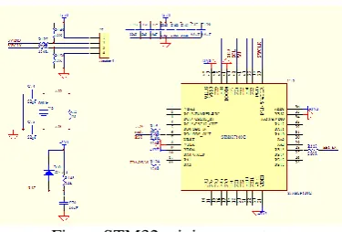
Figure STM32 minimum system
Figure 1 shows the composition of STM32 minimum system. The system regulation uses Serial Wire Debug (SWD) mode. According to the chip manual, connect Pin 37 and Pin 34 in STM 32 as per figure 1. STM 32 may be commissioned in SWD mode.
(2) RT9214 Voltage regulating circuit
In the design process of RT9214 voltage regulating circuit, we firstly analyze the classical circuit given in chip data, and calculate the output voltage. The classical power output circuit of RT9214 is shown in figure 2.
Figure 2 RT9214 Output circuit
Voltage regulation principle of RT9214: When the feedback pin receives the voltage VFB≤0.8 V, RT9214 widens the duty and increase the voltage. When VFB≥0.8 V, RT9214 narrows the duty and stabilize the voltage. In the regulation mode, according to the overlapping principle in circuit analysis, we derive the standard formula of circuit output voltage VO:
V R
R R
VO 0.8
2 1
1
(2)
It is organized from formula (2):
) 1 ( 8 . 0
1 2 R R V
VO (3)
Formula (3) is the calculation formula of output voltage standard given in RT9214 chip manual. The disadvantage of the circuit lines in regulating the output voltage through changing the proportion of two feedback resistance. It is inconvenient to use. We improve the circuit. The circuit is shown in figure 3.
Figure 3 The design of STM32 controlling the output
Where, Vc is the control voltage. When other parts of circuit are not changed, according to the circuit overlapping principle, we may obtain that:
V R
R R V
R R
R
VO C 2 0.8
2 1 2
1
1
www.ijeijournal.com Page | 30
It is organized:
V R R V R R
VO - C (1 ) 0.8
1 2
1
2
(5)
As shown in formula (5), output voltage is not only determined by the proportion of R2 and R1. It also relates to PWM control voltage given in STM32. At the same time, it is an inverse relation, namely when Vc is the maximum, the output voltage will be the minimum; when Vc is the minimum, the output voltage will be the maximum;
Here, the output voltage of embedded central control system is 0~+3.3V. The regulation amplitude of voltage is too low and it does not meet the requirements. It is too complex to regulate through the proportional relationship; therefore, we amplify PWM output of embedded central control system as voltage regulation Vc of RT9214. The circuit is shown in figure 4.
Figure 4 Amplified STM32 amplitude modulation circuit The circuit uses integration computing amplifier RT9214. The input in positive end refers to voltage Vref and the negative end inputs PWM voltage of embedded central control system. The output end connects the resistance about 5KΩ and achieves rail-rail output, making it accurately output 0V voltage under low-voltage output. The expression of voltage at output end is calculated with node overlapping principle:
C g f ref g f f
PW M V
R R Rg V R R R V
- (6)
It is organized:
ref g f PW M g f C V R R V R R
V (1 ) (7)
As shown in formula 97), the key point in Vc voltage control is divided into two parts: one part is the ratio of Rf and Rg; Vref is the fixed quantity of two systems, namely the parameter may not be adjusted when the system design is completed; another part is VPWM, namely PWM output waveform of STM32. It is the procedure control variable and the voltage regulation may be outputted according to the system requirement. The change in Vc amplitude may break the limitation of STM32 output 3.3V and design to the required size through calculating feedback loop proportion and referring to the voltage. In order to obtain the output voltage V0, formula (7) is substituted into formula (5).
) 1 ( 8 . 0 ) ) 1 ( ( -1 2 1 2 R R V R R V R R R R V ref g f PW M g f
O (8)
1 2 R R
is t,
g f
R R
is k, it is organized from formula (2):
) 1 ( 8 . 0 ) ) 1 (
( kV k V t
t
VO PW M ref (9) it is organized:
) ) 1 ( ) 1 ( 8 . 0 ( ref PW M
O tkV t t k V
V (10)
1. Experimental results
In order to verify the correctness and reliability of the design, the circuit parameters are designed and the results are in agreement with the calculated results. In the experiment, parameter t is set as 13.33,k is set as 0.255, Vref is 0.6 V. Substitute t, k and Vref into formula (9):
255 . 0 4
.
3
pwm
O V
V (11)
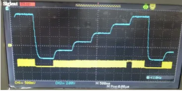
As shown in the above formula, the design relates to the quantity relationship between VPWM and RT9214 output voltage. The experimental results refer to figure 5:
Figure 5 Output waveform of
30% of PWM duty
Figure 6 Output waveform of duty 50% of PWM wave
Figure 7 Stepped output of PWM waveform forming of PWM circulation regulation
When figure 5 shows PWM wave duty is 30%, VPWM is 1.12 V and RT9214 output voltage is 3.84 V; figure 6 shows when PWM wave duty is 50%, VPWM is 1.64 V,RT9214 output is 5.76 V; substituting the data into formula (11), we may see the accuracy of formula. Figure 7 is adjusting PWM wave duty through cycle. RT9214 presents the waveform of stepped output. As shown in the figure, the output voltage of RT9214 changes according to the changes in PWM wave duty. The correctness of the design idea is proved by the formula calculation and experimental waveform. The design uses a PWM output pin in the STM32 with the RT9214 feedback voltage using the voltage divider principle, together with the control of the pin6 RT9214 feedback voltage to accurately control the output voltage.
III.
SUMMARY AND PROSPECT
www.ijeijournal.com Page | 32
mode of circuit parameters and flexibly applies RT9214 classical circuit and output characteristics, and extends the use scenario of RT9214.
REFERENCES
[1]. Hu Xiangjun, Circuit Analysis (edition II) [M]. Beijing: Higher Education Press, 2006
[2]. Wang Guan, Chen Jiankui, Zhai Jie, Shi Minghui, Temperature acquisition scheme based on amplifier and temperature sensor [J]. Instrument Technique and Sensor, 2014(11):66-69.
[3]. Li Dong, Lu Hongjuan: Analysis of Application Circuit in DC speed control system circuit [J]. Electronic Design Engineering 2012,20(2):181-183
[4]. Li Shuo, Dong Yiyuan, Design of overcurrent alarm device based on CSM020B and LM324 [J]. Modern electronic technology 2011,34(24):63-65.
[5]. RT9214-5V/12V Synchronous Buck PWM DC-DC Controller[R]. RICHTEK,2011
[6]. Tong Hua, Tong Jianzhong, Fault diagnosis and maintenance of computer mainboard [J]. Silicon Valley 2009(13):32
Author:
1. Wu Jun,1978, male, associate professor and doctor.
2. Wang Guoliang, 1991, male, Master Degree. The second author is communication author, School of electronic and information engineering, Tianjin University of Technology, No. 399, West of Binxi Road, Xiqing District, Tianjin City.