Design and Analysis of Low Power
Temperature Sensor using Static Latch D
Flip-Flop
Anurag Battu, K.Shriniwas Rao
M.Tech. (VLSI Design), Dept. of EC, Mewar University, Chitorgarh, Rajasthan
Assistant Professor, Dept. of EC, Mewar University, Chitorgarh, Rajasthan
ABSTRACT: This paper presents CMOS temperature sensor which is designed using static latch d flip-flop at 180 nm CMOS technology. CMOS temperature sensor also consists a voltage level shifter, a counter, and a register that is designed using d flip flop. Temperature sensor occupies smaller silicon area with higher resolution than the conventional temperature sensor. Used VCRO has full range voltage controllability along with a wide tuning range and is most suitable for low-voltage operation due to its full range voltage controllability. The frequency range of VCO is calculated as 185 MHz to 810 MHz by its characteristic, with frequency of 93 MHz. Power dissipation of Voltage controlled ring oscillator at 1.8 V power is 438.91µW. Various parameters like delay and power dissipation of other circuits are also calculated with respect to different power supply & threshold voltages.and Result shows that speed and power dissipation of circuit are directly proportional to power supply voltage. Power dissipation and delay of VCRO based temperature sensor at 1.8V power supply is 313.91 mW and 0.108nS respectively and temperature range is from -175 to +165.
I. INTRODUCTION
Fig.1. Block diagram of temperature sensor
II. DESIGN OF CIRCUIT
1. voltage controlled oscillator (VCO:
A voltage controlled oscillator (VCO) is one of the most important building blocks in analog and digital circuits. An oscillator is an electronic device used for the purpose of generating a specific frequency signal. The voltage controlled oscillator is the circuit block where the control voltage controls the oscillator’s output frequency so that it matches the reference signal frequency A ring oscillator consists of number of gain stages in a loop in which output of the last stage is fed back to the input of the first. The ring oscillator must satisfy the Barkhausen criteria, which says that it should
provide a phase shift of 2π and to achieve oscillation it must have a unity gain. The voltage controlled oscillator is designed using self-bias ring oscillator as shown in figure 2.
Fig.2. Voltage Controlled ring oscillator
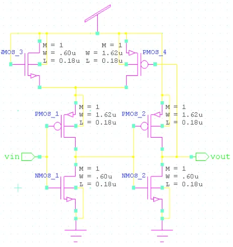
2. D Flip Flop
Fig.3. Schematic Diagram of D Flip- Flop
It consists 4 nand gate and 1 not gate. D and clk are its input. Clock pulse (clk) is used to control the data moving from input to output.
3. Level Shifter
In this temperature sensor the Voltage level shifter circuit converts low level input voltage to high level output voltage. Generated output voltage of a level shifter will be either less, greater than or equal to a given input voltage.Shifter use in the temperature sensor circuit increase the reduced voltage level of ring oscillator output to full scale n make persuaded that the number of its rising edge is counted in the counter. Schematic diagram of level shifter is shown in fig 4.
4. Temperature Sensor component and temperature Sensor
It consists of ring oscillator and a pulse counter circuit. Oscillation period (1/f) of voltage controlled ring counter is converted to a number of oscillations by applying enable signal of fixed pulse width, and the number of oscillations is stored in the counter to produce the digital output. Additional circuitry between enable input and the ring oscillator is used to remove synchronization problem, and the sensor outputs are connected to transmission gates to avoid unnecessary toggling. The reason of synchronization problem is the oscillator frequency which is temperature-dependent. Schematic diagram of Temperature Sensor component is shown above in fig. 5.
Fig.5. Temperature Sensor component
A temperature sensor is a device that gathers data concerning the temperature from a source and converts it to a form that can be understood either by an observer or another device. Schematic diagram of Temperature Sensor is shown above in fig. 6.
III. RESULT AND DISCUSSION
1. Ring Oscillator
The voltage controlled oscillator is used to generate a specific frequency signal. The VCO is designed by 3-stage ring oscillator which gives better VCO
Fig7. Voltage Controlled Ring Oscillator
Fig.8. Characteristic of VCO
characteristic and frequency range. The simulated waveform of VCO and the characteristic is shown above in fig 6 and fig 7.Power dissipation and delay of ring oscillator at different power supply voltage is shown below in table 1 when W/L ration of PMOS transistor is equal to 3 times of NMOS W/L ratio.
Table 1. Power Dissipation & Delay of Ring Oscillator at different Voltage
Vdd(V) Delay(nS) Frequency(MHz) Power
dissipation(µW)
1.8 0.108 810 313.91
1.6 0.121 613 2260.41
1.4 0.140 438 110.53
1.2 0.198 230 105.27
Here we see that by increasing power supply voltage delay of the circuit decreases while power dissipation increases as power dissipation of circuit is directly proportional to square of power supply voltage.
2. Level Shifter
Waveform of voltage level shifter is shown below in fig 9. When the input signal Vin is low then output will also low & if input signal Vin is high then the output will be high.
Fig.9. Waveform voltage level shifter
3. Temperature sensor
Ring oscillator-based temperature sensors provide a
good indication of circuit speed. Its waveform is shown below in fig 10.
Fig.10. Waveform voltage level shifter
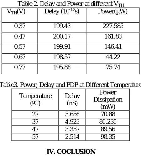
Table 2. Delay and Power at different VTH
VTH(V) Delay (10-15s) Power(µW)
0.37 199.43 227.585
0.47 200.17 161.83
0.57 199.91 146.41
0.67 198.57 44.22
0.77 195.88 75.74
Table3. Power, Delay and PDP at Different Temperature
Temperature (ºC) Delay (nS) Power Dissipation (mW)
27 5.656 70.88
37 4.923 80.235
47 3.357 89.56
57 2.514 98.35
IV. COCLUSION
A voltage controlled ring oscillator-based C MOS temperature sensor has been designed at 180 nm C MOS TSMC technology in Tanner Tool 13.1. smaller silicon area occupies by the proposed temperature sensor with higher resolution than the conventional temperature sensor based on band gap . The characteristic of VCRO is drawn between its control voltage and frequency.
ReferenceS
[1] Shruti Suman, Prof. B.P. Singh, “Ring Oscillator Based CMOS Temperature Sensor Design”, International Journal of Scientific & Technology, ISSN 2277-8616, Volume 1, Issue 4, May 2012.
[2] Stuart N. Wooters, Adam C. Cabe, Zhenyu Qi, Jiajing Wang, Randy W. Mann, “Tracking On-Chip Age Using Distributed, Embedded Sensors”, IEEE Transactions On Very Large Scale Integration (Vlsi) Systems, Vol. 20, No. 11, November 2012.
[3]David Wolpert, and Paul Ampadu, “Exploiting Programmable Temperature Compensation Devices to Manage Temperature-Induced Delay Uncertainty”, Ieee Transactions On Circuits And Systems—I: Regular Papers, Vol. 59, No. 4, April 2012.
[4]Oleg Garitselov, Saraju P. Mohanty, and Elias Kougianos, “A Comparative Study of Metamodels for Fast and Accurate Simulation of Nano-CMOS Circuits” IEEE Transactions On Semiconductor Manufacturing, Vol. 25, No. 1, February 2012.
[5]Ruxi Wang, Dushan Boroyevich, Puqi Ning, and Kaushik Rajashekara, “A High-Temperature SiC Three-Phase AC–DC Converter Design for >100 ◦C Ambient Temperature”, IEEE Transactions On Power Electronics, Vol. 28, No. 1, January 2013.
[6] Kisoo Kim, Hokyu Lee, and Chulwoo Kim “366-kS/s 1.09-nJ 0.0013-mm2 Frequency-to-Digital Converter Based CMOS Temperature Sensor Utilizing Multiphase Clock” IEEE Transactions On Very Large Scale Integration (Vlsi) Systems, Vol. 21, No. 10, October 2013.
[7] Michael H. Perrott, Haechang Lee, and Fari Assaderaghi, “A Temperature-to-Digital Converter for a MEMS-Based Programmable Oscillator With ˂ ±0.5-ppm Frequency Stability and ˂ 1-ps Integrated Jitter”, IEEE Journal Of Solid-State Circuits, Vol. 48, No. 1, January 2013.
[8] Hua Wang, Ching-Chih Weng, and Ali Hajimiri, “Phase Noise and Fundamental Sensitivity of Oscillator-Based Reactance Sensors”, IEEE Transactions On Microwave Theory And Techniques, Vol. 61, No. 5, May 2013.
[9] Nima Sadeghi, Alireza Sharif-Bakhtiar, and Shahriar Mirabbasi A 0.007- 108- 1-MHz Relaxation Oscillator for High-Temperature Applications up to 180 in 0.13- CMOS IEEE Transactions On Circuits And Systems—I: Regular Papers, Vol. 60, No. 7, July 2013.
[10] Xuehui Zhang and Mohammad Tehranipoor, “Design of On-Chip Lightweight Sensors for Effective Detection of Recycled ICs”, IEEE Transactions On Very Large Scale Integration (Vlsi) Systems.
[11] Clifton L. Roozeboom, Matthew A. Hopcroft, Wesley S. Smith, Joo Yong Sim, David A. Wickeraad, Peter G. Hartwell, and Beth L. Pruitt, “Integrated Multifunctional Environmental Sensors” Journal Of Microelectromechanical Systems, Vol. 22, No. 3, June 2013.
[12] Young-Jae An, Kyungho Ryu, Dong-Hoon Jung, Seung-Han Woo, and Seong-Ook Jung, “An Energy Efficient Time-Domain Temperature Sensor for Low-Power On-Chip Thermal Management”, IEEE Sensors Journal, Vol. 14, No. 1, January 2014.