Universal Current-Mode Biquad Filter Using a VDTA
Dinesh Prasad1*, Data Ram Bhaskar1, Mayank Srivastava2
1Department of Electronics and Communication Engineering, Faculty of Engineering and Technology,
Jamia Millia Islamia, New Delhi, India
2D/O Electronics and Communication Engineering, Amity School of Engineering and Technology,
Amity University, Noida, India
Email: *[email protected], [email protected], [email protected]
Received October 9,2012; revised November 9, 2012; accepted November 16, 2012
ABSTRACT
This paper presents a new current-mode single input multi output (SIMO) type biquad employing one voltage differ- encing transconductance amplifier (VDTA), two grounded capacitors and a single grounded resistor. The configuration realizes all basic filter functions (i.e. Low Pass (LP), High Pass (HP), Band Pass (BP), Notch (BR) and All Pass (AP)). The natural frequency (ω0) and bandwidth (BW) are independently tunable. The workability of proposed configuration has been verified using SPICE simulation with TSMC CMOS 0.18 μm process parameters.
Keywords: Current Mode Filter; Voltage Differencing Transconductance Amplifier
1. Introduction
Active filters are important basic building blocks, which are frequently employed in electrical engineering appli- cations. The current-mode approach [1] in designing ac- tive filters has become more popular due to its advanta- geous features such as larger dynamic range and wider bandwidth as compared to voltage-mode counterparts (particularly for the high frequency operations), simpler filtering configurations and lower power consumption. During the past few years, active filters using different current-mode/voltage-mode building blocks have been employed in which VDTA, recently introduced in [2], appears to be a useful active building block for an easy CMOS implementation of current-mode signal process- ing/signal generation [3-5].
Various SIMO-type active filters using different active elements are available in the literature see [6-13] and the references cited therein. In references [6-9], SIMO-type filter configurations employing 2/4 resistors and 2/3 ca- pacitors have been presented. These proposed filter struc- tures do not realize all the five filter responses. The con- figurations presented in [10] and [11] although use one resistor and two capacitors but fail to realize all the basic filter functions. Although the biquads proposed in [12] and [13] realize all the five filter functions but they use two capacitors along with 2/3 resistors. Therefore, the purpose of this communication is to propose a new SIMO-type current-mode universal biquad filter em- ploying one VDTA, two grounded capacitors and a sin-
gle grounded resistor, which realizes all the basic filter functions i.e. LP, HP, BP, BR and AP. The natural fre- quency ω0 and BW are independently tunable. The pro- posed circuit also offers low active and passive sensitivi- ties. The workability of proposed configuration has been verified using SPICE simulation with TSMC CMOS 0.18 μm process parameters.
2. The Proposed New Configurations
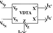
The symbolic notation of the VDTA is shown in Figure 1, where VP and VN are input terminals and Z, X+ and X− are output terminals. All terminals of VDTA exhibit high impedance values [2]. The VDTA can be described by the following set of equations:
1 1
2
2
0
0 0
0 0
P
N
m m V
Z
m V
X
m Z
X
g g V
I
I g V
g V
I
(1)
The proposed circuit configuration is shown in Figure 2.
A routine circuit analysis of Figure 2 yields the fol- lowing filter transfer functions:
1 21 1
m m o
LP in
g g I
T s (2)
I D s
1
1 2
2
m
o BP
in
g s
C I
T s
I D s
(3)
VP VD
VN Z X
X TA
IZ VP
V
VN
V
+
-IX+
IX
-VZ
Figure 1. The symbolic notation of VDTA.
R1
C1
V Z X
X
P
VDTA
VN +
-I01
Iin
C2 I02
I03
Figure 2. The proposed configuration.
o3
2in
I
3 HP
s T s
I D s
(4)
1 2
2 1 2
m m
g g s
C C
I D s
3 1 4
o o
NOTCH
in
I I
T s (5)
1 1 2
1 1 2
m m m
g g g
C C C
s
2
3 2 1
5
o o o AP
in
s s
I I I
T s
I D
(6) where
1 21 1 1 2
m m
2 1 g g C C
D s s s
R C
(7)
The natural frequency ω0, BW and quality factor Q0 are given by:
1 2
0
1 2
m m
g g C C
(8)
1 1 1
BW R C
(9)
and IB1 = IB2 = 150 μA, IB3 = IB4 = 42.38 μA biasing cur- rents are used. The passive elements of the configuration were selected as C1 = C2 = 0.01 nF and R1 = 1.58 KΩ. The transconductances of VDTA were controlled by bias currents. Figure 3 shows the simulated filter responses of LP, BP, HP, BR and AP. These results, thus, confirm the validity of the proposed configuration. A comparison with other SIMO-type current-mode biquads using a sin- gle active device is presented in Table 1.
4. Conclusion
A new current-mode SIMO-type biquad filter has been presented which uses only one VDTA and three ground- ed passive elements. The proposed filter can realize the second-order LP, BP, HP, BR and AP responses. The circuit employs all grounded passive components (which is desirable for IC implementation) and offers low active and passive sensitivities. The natural frequency (ω0) and bandwidth (BW) are independently tunable. SPICE simulations have established the workability of the pro- posed formulation.
1
102 103 104 105 106 107 108 109
0 0.1 0.2 0.3 0.4 0.5 0.6 0.7 0.8 0.9
HP
Frequency (Hz)
Cu
rren
t Ga
in AP
BP
LP
[image:2.595.128.218.86.142.2]BR
[image:2.595.310.534.355.519.2]Figure 3. Frequency response.
Table 1. Comparison with other SIMO-type current-mode biquads using a single active device.
Reference No. of active component resistors No. of capacitors No. of
All five filter function realized [6] 1 4 2 NO
[image:2.595.307.538.568.736.2]4. Acknowledgements
This work was performed at the Advanced Analog Signal Processing Laboratory of the Department of Electronics and Communication Engineering, F/o Engineering and Technology, Jamia Millia Islamia, Jamia Nagar, New Delhi-110025, India.
REFERENCES
[1] C. Toumazau, F. J. Lidgey and D. G. Haigh, “Analogue IC Design: The Current-Mode Approach,” Peter Peregrinus Limited, London, 1990.
[2] D. Biolek, R. Senani, V. Biolkova and Z. Kolka, “Active Elements for Analog Signal Processing, Classification, Review and New Proposals,” Radioengineering, Vol. 17, No. 4, 2008, pp. 15-32.
[3] A. Yesil, F. Kacar and H. Kuntman, “New Simple CMOS Realization of Voltage Differencing Transconductance Amplifier and Its RF Filter Application,” Radioengineer-ing, Vol. 20, No. 3, 2011, pp. 632-637.
[4] D. Prasad and D. R. Bhaskar, “Electronically-Controllable Explicit Current Output Sinusoidal Oscillator Employing Single VDTA,” ISRN Electronics, Vol. 2012, 2012, Arti-cle ID: 382560. doi:10.5402/2012/382560
[5] J. Satansup, T. Pukkalanun and W. Tangsrirat, “Electroni-cally Tunable Single-Input Five-Output Voltage-Mode Universal Filter Using VDTAs and Grounded Passive Elements,” Circuits, Systems, and Signal Processing, 2012 (online). doi:10.1007/s00034-012-9492-0
[6] A. Fabre and J. L. Houle, “Voltage-Mode and Current- Mode Sallen-Key Implementations Based on Translinear Conveyors,” IEEE Proceedings-G: Circuits, Devices and
Systems, Vol.139, No.7, 1992, pp. 491-497.
[7] C. M. Chang, C. C. Chien and H. Y. Wang, “Universal Active Current Filters Using Single Second Generation Current Conveyor,” Electronics Letters, Vol. 29, No. 13, 1993, pp. 1159-1160. doi:10.1049/el:19930775
[8] E. Yuce, B. Metin and O. Cicekoglu, “Current-Mode Bi-quadratic Filters Using Single CCIII and Minimum Num-ber of Passive Elements,” Frequenz: Journal of RF-En-gineering and Telecommunications, Vol. 58, No. 9-10, 2004, pp. 225-227.
[9] B. Chaturvedi and S. Maheshwari, “Current Mode Biquad Filter with Minimum Component Count,” Journal of Ac-tive and Passive Electronic Components, Vol. 2011, 2011, Article ID: 391642. doi:10.1155/2011/391642
[10]D. Biolek, V. Biolkova and Z. Kolka, “Current-Mode Biquad Employing Single CDTA,” Indian Journla of Pure and Applied Physics, Vol. 47, No. 7, 2009, pp. 535- 537.
[11]W. Tangsrirat, “Novel Current-Mode and Voltage-Mode Universal Biquad Filters Using Single CFTA,” Indian Journal of Engineering and Material Science, Vol. 17, 2010, pp. 99-104.
[12]C. N. Lee and C. M. Chang, “Single FDCCII-Based Mixed-Mode Biquad Filter with Eight Outputs,” AEU: International Journal of Electronics and Communications, Vol. 63, No. 9, 2009, pp. 736-742.
doi:10.1016/j.aeue.2008.06.015
[13] D. Prasad, D. R. Bhaskar and A. K. Singh, “Universal Current-Mode Biquad Filter Using Dual Output Current Differencing Transconductance Amplifier,” AEU: Inter-national Journal of Electronics and Communications, Vol. 63, No. 6, 2009, pp. 497-501.
Appendix: Non-Ideal Analysis
Considering the non-ideal effect of various parameters of VDTA i.e., the finite X-terminal parasitic impedance consisting of a resistance X in parallel with capaci- tance X , the parasitic impedance at the Z-terminal consisting of a resistance
R C
Z
R in parallel with capaci- tance CZ, the parasitic impedance at the Vp-terminal consisting of a resistance Rp in parallel with capaci- tance Cp
R C
and the parasitic impedance at the Vn-terminal consisting of a resistance n in parallel with capaci- tance n. The parasitic impedances belong to the circuit shown in Figure 2 are indicated in Figure A1.
Considering the above parasitic impedances, the natu- ral frequency ω0 and quality factor Q0 are found to be:
1 2
2
m m
1 0
1 2 1 2
1 1 1 1
x n z
z x z x
R R R R
C C C C C C C C
n n z
g g
C C C C
R1
C1
V Z X
X
P VDTA VN
(a)
+
-I01 Iin
Rx
Cx
Rn Cn
C2 I02
I03
Cz Rz
[image:4.595.320.515.80.282.2]Rp Cp
Figure A1. Parasitic impedances of VDTA affecting the circuit of Figure 2.
1 2 1 2 1 2 2
1 2 2 2
1 1
1 1
m m z x z x n n z
z
x n z z z
z z z x x n n
1 0
1 1
x n
g g C C C C C C C C C C C C
R
C C
C C C C C C C
R R R R R R R R R
R R R
Q
(b)
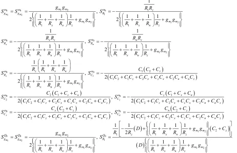
The sensitivity of ω0 and quality factor Q0 with respect to its active and passive elements are given as:
1 2
0 0 0
1
1 2
1 2 1 2
0 0
1 2 1
1
1 1
1 1
1
,
1 1 1 1 1 1 1 1
2 2
1 1
,
1 1 1 1 1 1 1 1
2 2
m m
x n
m m z
g g R
m m m m
x n z x n z
x z n z
R R
m m m
x n z x n z
g g R R
S S S
g g g g
R R R R R R R R
R R R R
S S
g g g g
R R R R R R R R
2
2
1 1 1 1
m
n n z
x n
R R R R C C C
C C C
C C
0 0
1
1 2
0 0
1 1 2
1 2 1 2
1
2 1 1
,
2
1 1 1 1
2
,
2 2
z
z x n z
R C
z x z x m m
x n z
x n z
C C
S S
C C C C C C C C C
g g
R R R R
C C C C C C
S S
C C C C C C C C C C C C C C C C
[image:4.595.70.532.433.732.2]
1 2 0
1 2
1 2 0
1 2
2 1
1
2 1
1
1 1 1 1 1 1
2
,
1 1 1 1
1 1 1 1 1 1
2
1 1 1 1
x
n
m m z
x z x n z
Q R
m m
x n z
m m z
n z x n z
Q R
m m
x n z
D g g C C
R R R R R R
S
D g g
R R R R
D g g C C
R R R R R R
S
D g g
R R R R
1 2 0
1 2
0 0
1 2
1
1 1
1
2 1 1 2
1 ,
1 1 1 1 1 1 1 1 1
2
1 1 1 1
1 1
1 1
2 2
, z
m m x
z x n x n z
Q R
m m
x n z
x n
z
z
Q Q
C C
D g g
R R R R R R R R
S
D g g
R R R R
C C C C D E
C C C D E
R
S S
D E
,
1 1
n
x n
C C C
R R R
0 0
0
1 2
1
2
1 1 1 1
2 2
1 1
2
,
z x
n
z x n x z
x n
Q Q
C C
n z p
z Q
C
D E
C C C C D E C C C
R R R
S S
D E D E
C C C C D E
R S
D E
,
1 1
, z ,
D E
R
(c)
where
1 2 2 2
1 2 1 2 1 1
x n z z z
z x z x
z z z x x n n
C C
C C C C C C C
D E C C C C C C C C C
R R R R R R R R R
,
2CnC Cn z
. (d)From the above mentioned sensitivity values, it is easy to figure out that all the active and passive sensitivities