Rochester Institute of Technology
RIT Scholar Works
Theses
7-2019
Design of a Multiband Stacked Microstrip Patch
Antenna for Satellite Communications Application
Hadef Ahmed Alshamsi
Follow this and additional works at:https://scholarworks.rit.edu/theses
This Thesis is brought to you for free and open access by RIT Scholar Works. It has been accepted for inclusion in Theses by an authorized administrator of RIT Scholar Works. For more information, please [email protected].
Recommended Citation
Design of a Multiband Stacked Microstrip Patch Antenna for
Satellite Communications Application
by
Hadef Ahmed Alshamsi
A Thesis Submitted in Partial Fulfillment of the
Requirements for the Degree of Master of Science in Electrical Engineering
Department of Electrical Engineering and Computing Sciences
Rochester Institute of Technology – Dubai
Dubai – UAE
II
Design of a Multiband Stacked Microstrip Patch Antenna for
Satellite Communications Application
by
Hadef Ahmed Alshamsi
A Thesis Submitted in Partial Fulfillment of the Requirements for the Degree of Master of Science in Electrical Engineering Department of Electrical Engineering and Computing Sciences
Approved by:
__________________________________________________________________Date:______________
Dr. Bouthaina Talili
Thesis Advisor – Department of Electrical Engineering and Computing
__________________________________________________________________Date:______________
Dr. Adbulla Alzarouni
Thesis Committee Member – Department of Electrical Engineering and Computing
__________________________________________________________________Date:______________
Dr. Jinane Mounsef
Thesis Committee Member – Department of Electrical Engineering and Computing
III
Abstract
IV
Table of Content
List of Figures ………..……….. VI
List of Tables ………..……… XI
List of Terminologies and Symbols ………..……… XII
Acknowledgement ………... XIII
Chapter I ……….………..…….………. 1
Introduction …………..………..………...…………. 1
Chapter II ………..…...…….……….. 3
Satellite Communication ……….………..………. 3
Chapter III ………..………..….….………. 7
Microstrip patch antenna ………..………. 7
3.1Antenna Parameters …..……….….………. 8
Chapter IV ……….…………. 12
Literature Review ……….……..……… 12
4.1Single Patch ………..……….………….. 13
4.1.1 Slots on the radiating element ……… 13
4.1.2 Feeding methodology ………. 19
4.2 Multiple Patches ………...……… 22
4.3 Multiple Patches with air gap ………..………. 33
4.4 Antenna performance enhancements techniques ………..……… 41
Chapter V ………..………..…….. 49
V
5.1Sample antenna design using ADS ……… 49
Chapter VI ………..……….. 58
Design of a Multiband Stacked Microstrip Patch antenna for Satellite Communications ……….…….. 58
6.1Design of Simple Microtsrip Patch antenna that radiates at 1.6 GHz … 59 6.2Improving the antenna bandwidth at the resonant frequency …….…... 72
6.3Modification to the antenna to obtain more resonant frequencies ….… 82 6.4Antenna Final Design ……….… 96
Chapter VII ……….……….……… 105
Conclusions
and further work
……….……….………. 105VI
List of Figures
Fig.1, Simple structure of patch antenna [2] ……… 8
Fig.2, Side view of patch antenna [2] ……….. 8
Fig.3, Design of the patch antenna [3] ………. 14
Fig.4, Dimensions of the patch antenna [3] ………. 14
Fig.5, Upper band Axial Ratio [3] …………..……….…… 15
Fig.6, Lower band Axial Ratio [3] ………..……… 15
Fig.7 Top of the patch antenna [4] ……...……..……….………. 15
Fig.8 Bottom of the patch antenna [4] ……..………...……… 15
Fig.9 Impedance bandwidth at the operating frequency [4] ……..……….. 16
Fig.10 Circular patch antenna with two circular slots [5] ………..……….. 17
Fig.11 Axial ration bandwidth of the circular patch [5] ………..……… 17
Fig.12 Designed antenna with 4 arc slots [6] ……….………. 18
Fig.13 AR bandwidth of the two operating bands [6] ………..………... 19
Fig.14 Square patch antenna and location of CP feeding [7] ………..………….………... 19
Fig.15 Antenna design [7] ………..………. 20
Fig.16 Return loss and impedance bandwidth [7] ………..………. 20
Fig.17 Designed stacked antenna [9] .………..………..……….. 23
Fig.18 Stacked antenna parameters [9] ………....……….……... 24
Fig.19 S-Slot patch [9] ………..………... 23
Fig.20 Ground plane [9] ………..………. 24
VII
Fig.22 Axial Ratio of the antenna [9] ………..……… 25
Fig.23 Dimensions of the designed antenna [10] ………. 25
Fig.24 Obtained results of the proposed antenna [10] ……….…………..………..… 26
Fig.25 Antenna structure of the work in [11] ……….……..………... 26
Fig.26 Antenna structure of the work in [12] ……….………..………... 26
Fig.27 The Axial Ration bandwidth of the antenna [12] ………..………... 27
Fig.28 Proposed patch antenna with multiple patches [13] ………. 28
Fig.29 Two half annular ring antenna [14] ……….. 29
Fig.30 Dimensions of the proposed antenna [14] ……….………..………. 29
Fig.31 Antenna impedance BW [14] ……….…………..……… 30
Fig.32 Structure of the proposed antenna in the work [15] ………. 31
Fig.33 Proposed antenna impedance BW [15] ……….…………..………. 32
Fig.34 Proposed antenna gain [15] ……….………..………... 32
Fig.35 LHCP with Coaxial Feed [16] ……….. 34
Fig.36 RHCP with side TL Feed [16] ……….. 34
Fig.37 Antenna design in the work [16] ……….. 35
Fig.38 Antenna design parameter of the work [16] .………..……….. 35
Fig.39 CP AR bandwidth of the antenna in the work [16] ……….. 35
Fig.40 Antenna design with cross slots of the work [17] ………..………. 36
Fig.41 Single patch of the designed array by the work in [18] ………..………. 37
Fig.42 The design of the proposed array by the work in [18] ..………... 37
Fig.43 Axial Ratio bandwidth of the designed array [18] ………... 38
VIII
Fig.45 The proposed antenna with thin substrate in the work [20] ..……….. 40
Fig.46 Antenna design considering single feed of the work [21] ..………. 41
Fig.47 Antenna design with differential plates feeding by the work [22] ..……… 42
Fig.48 Antenna design and dimensions [23] ……… 43
Fig.49 Antenna design with fractal E-shaped [24] ……….. 44
Fig.50 Antenna with DGS and Cavity Structure [25] ……….……… 46
Fig.51 Array Antenna with three DGSs [26] ……….………. 46
Fig.52 Antenna design with Cross slots and SMSH [27] ……… 47
Fig.53 Schematic workspace of ADS .………. 50
Fig.54 Defining the Sectional layers of the antenna ……… 51
Fig.55 Antenna of work [28] ………..………. 52
Fig.56 Sample Antenna (example) is placed in the layout plane ..……….. 52
Fig.57 Results of the antenna in [28] ………..……….…… 53
Fig.58 Results of the simulated example antenna ……… 54
Fig.59 Surface current of the example antenna ………... 55
Fig.60 Radiation pattern of the example antenna ……… 55
Fig.61 Different parameters of the example antenna ………..…… 56
Fig.62 Gain and Directivity of the example antenna ……….. 56
Fig.63 Absolute Fields of the example antenna …..……… 57
Fig.64 Axial Ratio and the Polarization of the example antenna ……… 57
Fig.65 Simplest rectangular antenna ……… 62
Fig.66 Return Loss of the simple rectangular antenna ……… 63
IX
Fig.68 Return Loss of the simplest square antenna ……….… 64
Fig.69 45 x 45 mm Antenna with corner cuts to achieve circular polarization …………...…… 66
Fig.70 LineCalc tool in ADS to find the length of the Feeding line ……… 67
Fig.71 Proposed with extended feeding line ……… 68
Fig.72 Antenna with inset matching line ………. 68
Fig.73 Return loss of antenna in Fig.71 ………... 69
Fig.74 Return loss of antenna in Fig.72 ………... 69
Fig.75 Axial Ratio of the simple antenna ……… 70
Fig.76 Return loss of the simple antenna from 0.5 GHz to 6 GHz ………. 71
Fig.77 Two patch antenna cross section ……….……… 73
Fig.78 Schematic of the two patch antenna ………..……….. 73
Fig.79 Return loss of the two patch antenna ……… 74
Fig.80 Surface Current of the electromagnetically coupled two patches ……… 75
Fig.81 Antenna cross sections with VIA being added between the two patched ……… 76
Fig.82 Schematic of the VIA ………... 76
Fig.83 Return loss of the Antenna with VIA between the two patches ………... 77
Fig.84 Antenna with Left VIA, and increased VIA conductor size ………. 78
Fig.85 Antenna with Right VIA, and increased VIA conductor size ……..……… 78
Fig.86 Left VIA return loss ……….. 79
Fig.87 Right VIA return loss ………... 79
Fig.88 Left VIA surface current ………... 80
Fig.89 Right VIA surface current ……… 81
X
Fig.91 Return Loss of the antenna in Fig.90 at 1.5 GHz frequency ……… 84
Fig.92 Upper patch much smaller than lower patch ……… 85
Fig.93 Return loss of the antenna proposed in Fig.92 ………. 86
Fig.94 Antenna with two VIAs ……… 87
Fig.95 Return loss of the antenna with two VIAs ……… 87
Fig.96 Slots on the upper patch ……… 88
Fig.97 Return loss of the antenna having a lot in upper patch ………. 89
Fig.98 Cross section of the antenna with 2.5 mm upper substrate thickness ……….. 90
Fig.99 Return loss of the Antenna in Fig.98 ………..……….. 90
Fig.100 Helix upper patch ………..………. 91
Fig.101 Return Loss of the Helix upper patch at the resonant frequency …..………. 92
Fig.102 Return Loss of the antenna with 2nd VIA higher than the center line ……… 93
Fig.103 Return Loss of the antenna with 2nd VIA along the center line ………. 94
Fig.104 Return Loss of the antenna with 2nd VIA lower than the center line ………. 94
Fig.105 Final Antenna layout with 2nd VIA lower than the center line ………... 95
Fig.106 Final Antenna Cross Section ……….. 96
Fig.107 Final Antenna Layout and dimensions ………... 97
Fig.108 Return loss of the Final Antenna from 1 GHz till 3GHz ……… 98
Fig.109 Return loss from 3 GHz till 6 GHz ………. 99
Fig.110 Axial Ratio of the Final Antenna Vs. Frequency ………..……... 100
Fig.111 Radiation Pattern of the Final Antenna at 1.487 GHz ………..……… 101
Fig.112 Surface current on top of the upper patch of the Final Antenna at 1.487 GHz …..….. 101
XI
List of Tables
Table.1 Comparison between different satellite communication companies [1] ………. 6
Table.2 Dimensions of the designed antenna [7] ………..……….. 20
Table.3 Final Antenna Dimensions ……….. 97
XII
List of Terminologies and Symbols
AR
Axial Ratio
CP
Circular Polarization
MS
Microstrip
Eq
Equation
FR_4
Dielectric Material (Substrate) with electric permittivity 4.6
Sat
Satellite
dB
decibels
Fig.
Figure
VIA
Vertical Interconnect Access
ADS
Agilent’s Advanced Design System 2011 Software
Er
Electric permittivity of a material
E
effEffective Dielectric Constant
GEO
Geosynchronous earth-orbit
MEO
Medium earth-orbitXIII
Acknowledgement
Chapter I
Introduction
In the last two decades, there have been huge developments in the communication field. From phones to mobile phones up to smart phones in the recent years, the rapid improvements show the amount of researches and enhancements in this field. The accessibility and the usage of the mobile networks and the internet are very critical in almost all the fields like education system, in businesses, in medicine, in space, in oil and gas and many other fields. Therefore, the continuous development in the communication field and its infrastructure is equally important. Looking at the size of the planet and the various scattered human concentrations, rural areas and industries, and vast ocean ships and vessels, makes it very difficult to cover all of these areas with landline communications infrastructure and provide direct access to the different users. As a result, many companies have introduced the idea of the satellite communications in order to overcome the shortcuts that land infrastructure cannot cover and develop.
2
Therefore, in our research we are exploring the different solutions to the antenna
requirements of the satellite communications taking into consideration the recent developments and requirements in the handheld devices like the compatibility, ease of fabrication and
integration. This thesis proposes a stacked microstrip patch antenna that can be used for satellite communication as well other communication purposes.
3
Chapter II
Satellite Communication
4
In satellite communication, there are also different types or categories that have to be defined. Mainly, there are three different levels or types of satellite communication antenna which are defined based on the attitude from the earth and the size of the foot print that it can cover on the earth. These three levels are GEO, Geosynchronous earth-orbit, MEO, Medium earth-orbit, and LEO, Low earth orbit [1]. GEO satellites are based from 35800 Km above the equator and higher [1]. GEO satellites can cover one third of the planet. Therefore, three GEO satellites equally spaced can cover the whole planet [1]. The main downfall of these satellites, is the lengthy path that the signal has to propagate through from the hand held device or the phone all the way to the satellite antenna and again back to the other side of the communication. These lengthy paths will affect the delay of the communications, and sometimes the loss of the
communications due to attenuation. MEO satellites are placed from 5000 Km up to 12000 Km above the equator [1]. More satellites and antennas are needed to cover the whole planet, but the path and the signal propagation are much less than that of the GEO satellite signals. LEO
satellites which are the closest to the planet are placed from the height of 500 Km up to 1500 Km above the earth [1]. More and more antennas are needed to cover the whole planet by the LEO satellites because of the smaller footprint that it can cover on the planet. Moreover, the
communication system is not easier as it though comparing to the GEO satellite specially if the two points of communications are far apart and the signals has to propagate through different LEO satellites. Therefore, there are delays in terms of the switching and signals propagating from LEO satellite to another rather than the lengthy path that is caused by the GEO satellite. As a result different companies considered different types of the satellite antennas, different
5
Furthermore, there are other issue and challenges the companies and manufacturers of the satellite communications face. The designs of the mobile set itself became more and more
6
Table.1 Comparison between different satellite communication companies [1]
System
name Iridium Globalstar ICO Ellipso
Asian Cellular
System ACeS
Thuraya
Orbit LEO LEO MEO LEO GEO GEO Primary
Services Voice, DATA, FAX
Coverage Worldwide Asia Pacific
Middle east, central Asia, India, and East Europe Initial Launch / start of service
1997 / 1998 1998 / 1999 1998 / 2000 2000 / 2000 1999 / 1999 2000 / 2000
System Cost 4.4 billion $ 2.6 billion $ 4.5 billion $ 1.1 billion $ 1 billion $ 1.2 billion $ Satellite
aloft 66 48 10 14 1 plus spare 1 plus spare Orbit, Km 780 1400 10355 8040 35800 35800
Satellite lifetime, years
5-8 7.5 12 5-7 12 15
Handset supplier Motorola, Kyocera Qualcomm, Telital, Ericsson Mitsubishi, NEC, Samsung, Erricsson, Panasonic L3
communications Ericsson
7
Chapter III
Microstrip patch antenna
Microstrip patch antennas have been very promising antennas especially in the telecommunications field. They are easy to design, to implement, and cheap to manufacture. They are very compact with the mobile phones design profile, and the performance of these antennas in the past decade has proven its promising future in the mobile communications fields as well as the distributed antennas field. Furthermore, it is much easier to implement one patch antenna in a mobile devise than having multiple patch antennas in mobile devices.
8
Fig.1 Simple structure of patch antenna [2] Fig.2 Side view of patch antenna [2]
3.1Antenna Parameters:
It is important to define different antenna parameters that describe the antenna to be studied or explored. The following are the main antenna parameters that need to be defined before proceeding into the literature review and antenna design:
A- Radiation Patterns:
9
1- Isotropic:
Isotropic radiation pattern is defined as “a hypothetical lossless antenna having equal radiation in all directions” [2]. Since it does not exist in reality, but taken as a reference for other directional antennas.
2- Directional:
Directional radiation pattern is defined as “having the property of radiating or receiving electromagnetic waves more effectively in some directions than in others” [2].
3- Omni-directional:
Omni-directional radiation pattern is a special type of the directional radiation patter and it is defined as “having as essentially non-directional patter in a given plane and a directional pattern in any orthogonal plane” [2].
B- Gain:
There are two main definitions of the antenna gain which are the Absolute Gain and the Relative Gain. Absolute Gain is defined as “the ratio of the intensity, in a given direction, to the radiation intensity that would be obtained if the power accepted by the antenna were radiated isotropically” [2]. On the other hand, Relative Gain is “the ratio of the power gain in a given direction to the power gain of a reference antenna in its referenced direction” [2].
Gain Equation:
Gain = 4π
, where
(1)10
C- Input Impedance:
The input impedance of the antenna is defined as “the impedance presented by an antenna at its terminals or the ratio of the voltage to current at a pair of terminals or the ratio of the
appropriate components of the electric to magnetic fields at a point” [2]. It is very important to have a good matching between the feeding lines to the antenna and the antenna in order to have a maximum power transferred to the antennas.
D- Return Loss:
Return loss is one of the most important parameters of an antenna. It basically represents the ratio of the power reflected from a port to that incident power into the port. As the return loss decreases that means the majority of the signal have propagated into the port or the antenna, hence there is a good matching.
Return Loss = - 20 Log |Γ | , where Γ is the reflection coefficient. (2) E- Bandwidth:
11
F- Polarization:
Polarization of an antenna is “in a given direction, the polarization of the wave transmitted (radiated) by the antenna” [2]. For more practical definition, the polarization is defined as “that property of an electromagnetic wave describing the time varying direction and relative magnitude of the electric-field vector”[2]. Polarization of the antenna or a wave can be categorized into three main polarizations which are linear, circular, and elliptical. Axial Ratio is a parameter that is used to define the polarization of an antenna or a wave. Axial Ratio “AR” is defined as the ratio of the major axis of the wave to the minor axis. Therefore, Axial Ratio falls in the following range: 1 ≤ AR ≤ ∞
1- Linear polarization: when there is no minor axis or very small comparing to the major axis, then AR is ∞.
2- Circular polarization: when the minor and the major axis are equal. Therefore, AR = 1 when there is a circular polarization. However, for practicality, AR = 3dB or less is considered acceptable to consider the wave or the antenna having circular polarization.
12
Chapter IV
Literature Review
In the literature review, the latest researches, journals, and studied around the globe related to this thesis were explored. Since, satellite communications and Microstrip patch antenna were presented earlier, the following literature review will focus on the Circular
Polarization of the antenna and different enhancement techniques that can be used to enhance the performance of the antenna for different other parameters like matching bandwidth or center frequency location. Many studies focused on obtaining circular polarization for microstrip patch antennas. Therefore, our following literature review will present the different studies categorized on four sections which are:
1- Single Patch: Focuses on the antennas that achieved CP with a single Microstrip Patch antenna.
2- Multiple Patch: Focuses on the antennas that achieved CP with Multiple Microstrip Patch antennas.
3- Multiple Patches with Air Gap: Focuses on the antennas that achieved CP with Multiple Microstrip Patch antennas with an air gap in between.
13
4.1 Single Patch
To achieve Circular polarization there are many ways, but the most important point is the ability to create a disturbance on the surface patch that will lead to a radiation that is of circular polarization. The disturbance is to make the antenna radiates two degenerate modes at the same magnitude but with 90 degrees phase shift between these two modes. Therefore, the disturbance that is to happen to the antenna surface will cause one of the two modes to start radiating at a different frequency which is a lower frequency level. Single patch antenna has been in studies in order to be used for Circular Polarization. That is, to use a simple patch antenna with two
metallic surfaces one as a patch surface and one as a ground and between the two plates is the dielectric material. Despite the many disadvantages of the single patch like the leakage current, the narrow impedance bandwidth, and very narrow CP Band width, it is more preferable by the industries and the manufacturers since it is easy to design, manufacture, and having
comparatively smaller thickness specially for hand held devices where the size is of high consideration. Therefore, many techniques were introduced in order to improve the
characteristics of the single patch antenna to be suitable and more practical to serve the type of radiation, the bandwidth, and the gain of the antenna. In the following discussion two types of the main techniques will be considered that are slots on the radiating element and feeding methodology.
4.1.1 Slots on the radiating element:
14
performance and radiation of the antenna. If the alternation is well designed and implemented, it would lead the patch antenna to radiate a circular polarization pattern. In [3], the author
presented a square patch antenna that will have a dual-band CP radiation performance. The CP was obtained by etching a rectangular slot at the center of the and by modifying the location of the feeding transmission line as in Fig.3 and Fig.4.
Fig.3, Design of the patch antenna [3] Fig.4, Dimensions of the patch antenna [3] After designing the patch antenna, eight extra slots where added to enhance the
15
order to achieve the circular polarization. Since the ground plane have a major effect on the antenna behavior in general and the radiation and its efficiency in particular,
Fig.5, Upper band Axial Ratio [3] Fig.6, Lower band Axial Ratio [3] the ground plane was reduced. In order to compensate for the effect of the reduction of the ground plane, two square slots were etched in the ground plane as in Fig.8.
16
Introducing slots in the ground plane will affect the performance of the antenna in terms of the input impedance, radiation pattern and the AR. As a result, an optimization study carried out in order to choose the best performance of the antenna as it shown in Fig.9. Despite the good performance of the antenna in terms of AR, impedance matching, and radiation pattern of the antenna, still the bandwidth of the operating frequency is narrow since it is only 3% impedance bandwidth.
Fig.9 Impedance bandwidth at the operating frequency [4]
In the same content, other researchers investigated the possibility to create a CP radiation antenna using two or more slots. The work in [5], circular polarization radiation pattern was achieved by using two circular slots etched on the radiation surface of the antenna. The
17
on the patch antenna since the AR can be reach up to 0.5 dB [5]. However, the main disadvantage of this design is the bandwidth of the designed antenna, since the achieved bandwidth is up to 28 MHz as it shown in Fig.11. The success of the concept of adding two circular slots on the patch to achieve CP, havs led other researchers to investigate more shapes and number of slots that can be added to the patch in order to achieve circular polarization. In a goal of achieving dual-band Circular polarization, the work in [6] proposes to use four arc slots
Fig.10 Circular patch antenna with two circular slots [5]
Fig.11 Axial ration bandwidth of the circular patch [5]
18
linear polarization, the dimensions and the locations of the arc were modified to satisfy the needed radiation polarization. Moreover, in one of the arcs a perturbation lot were added to achieve the best performance of the antenna [6]. In addition, the location of the feeding point on the antenna was chosen in two locations one to operate the antenna in a LH-CP and the other point is to operate the antenna as a RH-CP antenna as in Fig.12. It is important to note that, the two subtending angles play a great role in the CP achieved in the two bands. Moreover,
modifying the length and width the protruding slot has an effect in adjusting the operation frequency of the first mode and slightly affecting the other more.
Fig.12 Designed antenna with 4 arc slots [6]
19
Fig.13 AR bandwidth of the two operating bands [6] 4.1.2 Feeding methodology:
Another method to obtain a circular polarization for a single patch antenna is the location of feeding. It is well known that is feeding a square patch antenna at the corners of the antenna will lead to have a circular polarization. Choosing different corners to feed the patch antenna will result if different circular polarization either right handed or left handed as in Fig.14 [7].
Fig.14 Square patch antenna and location of CP feeding [7]
20
terms of the AX bandwidth, antenna gain, and different operation frequencies. In [7], the same principle was used in order to obtain dual-band CP operation. Therefore, a matching network as in Fig.15 has been used in order to operate the antenna at the two different frequencies [7].
Table.2 Dimensions of the designed antenna [7]
Fig.15 Antenna design [7]
The results of the designed antenna shows a good match between the concept and the
implementations. The antenna is reported to have a good impedance bandwidth that serve the purpose of the design as in Fig.16 [7].
21
From the proceeding, we can conclude that the single patch is very simple in terms of designing, manufacturing, and integrating with other microwave circuitry components.
Moreover, it has relatively smaller size in term of the thickness as long as the hand set devices are considered. However, there are other disadvantages that are associated with the single patch that makes the choice of this type of antenna not preferred in certain applications. One of the main disadvantages of the single patch antenna is the relatively small bandwidth of the 3 dB axial ratio. The smaller the bandwidth, the limited application choices of the antenna. The main reason for the smaller bandwidth is the thickness of the substrate, since smaller substrate leaks more current towards the ground plane, and hence the radiated signal is decreased. This problem can be avoided by different means, one of which using multiple antennas as an array where each antenna is radiating CP at a certain desired frequency. On the other hand, other problems
22
4.2 Multiple Patches
Given that the circular polarization can be achieved in many different ways like almost square patch antenna, slots in the patch antenna, double feeding network that feeds the patch antenna, and many other techniques, still the problems associated with the microstrip antennas cannot be neglected or solved by the simple antenna design. Therefore, many other techniques are being studied in order to improve the microstrip antenna performance in terms of the circular polarization axial ratio bandwidth, impedance bandwidth, constant gain level, and lower cross polarizations. One of the main fields of the improving techniques was discussed in the first section where the improvements are implemented on the main designed antenna. On the other hand, other main fields that are being considered in order to overcome the some of the problems associated with the single patch antenna that cannot be solved. One of these fields is the stacked patch antenna, where there is two substrates are being used in order to improve the antenna performance. Using two substrate can improve the antenna performance greatly in term of the operating bandwidth, lower cross polarization, better antenna gain and efficiency [8]. The reason behind this improvement is due to the fact that two different substrates will eventually operate as a material of permittivity that is between the two materials’ permittivity called effective
23
the top patch antenna is coupled to the feeding network. This method of feeding network will reduce the surface waves greatly since there is no direct feed to the patch and hence improving the antenna efficiency [8]. In addition to that advantage, another antenna can be implemented in between the two substrates which will make the antenna perform better than a single patch antenna. For these reasons, stacked patch antennas became a very attractive field for
investigations and implementations in many applications. In [9], the principle of the stacked patch antenna is demonstrated where the antenna is designed of two substrates and three conducting materials. Looking at the cross section of the antenna, it consists of a top conductor that will be the patch antenna, then the substrate, ground plane, another substrate, and the feeding line is on the back of the patch antenna. On the top patch antenna, an S-shaped etch is made in order to achieve circular polarization performance [9]. Moreover, it is found that loading the antenna with two slots at the edge of the radiating element will operate the antenna in dual frequency bands. Therefore, the s-shaped slot will result in a dual band circular polarization performance [9].
24
Fig.18 Stacked antenna parameters [9] Fig.20 Ground plane [9] On the ground plane, a rectangular slot is etched in order for the waves to be coupled with the top patch antenna. The advantage of using the coupling feeding methodology is reducing the surface waves on the top of the patch antenna, which is related inversely with the efficiency of the radiated signal, hence improving the efficiency of the antenna. The upper substrate is chose to be of lower dielectric material to increase the coupling of the patch antenna as shown in Fig.17, Fig.18, Fig.19, Fig.20 [9]. The results of the designed antenna show a good performance in terms of the gain, dual-band circular polarization performance as in Fig.21 and Fig.22 [9]. However, the disadvantage of the proposed is in the narrow bandwidth of performance.
25
Fig.22 Axial Ratio of the antenna [9]
Similarly, [10] proposes a single feed antenna with stacked patches in order to achieve circular polarization radiation pattern. However, the designed antenna has a different feeding
methodology where the coaxial probe is feeding the lower antenna as in the Fig.23, and hence the top patch is coupled with the lower patch [10]. The sizes of the two patches and the location of the feeding point has been optimized in order to achieve the best circular polarization
radiation pattern with the highest bandwidth possible. The results of the designed antenna as in Fig.24, shows that AR of 2.5 dB is achieve over more than 13% bandwidth typically acceptable [10].
26
Fig.24 Obtained results of the proposed antenna [10]
Likewise, two works as in [11] and [12] proposes to use three substrates with the designed antenna. The third material that has been added which is having relatively lower permittivity. However, the location of the feeding point and the order of the layers are different in the two designs as it is shown in Fig.25, and Fig.26 [11], [12]. Both antennas have been designed by optimization where the location of feeding point and the thickness of the substrates have been optimized in order to achieve the best antenna performance.
27
The results of the designed two antennas, proves the validity of the concept, where the antenna operates at a relatively high bandwidth as in Fig.27 [12].
Fig.27 The Axial Ration bandwidth of the antenna [12]
The principle of the stacked patch antenna can be extended to a wider range of different designs and antenna configurations. One of the examples is using more than two patches and a ground, in which multiple layers of substrates and patches are used. This is could have been used in order to operate the antenna in more than one band, or to improve the antenna performance in a certain band. Reference to the work in [13], the author designed an antenna that consists of three patches, ground plane, four substrates, and a feeding network. The proposed design is intended to operate at a three different bandwidths with a circular polarization. The feeding methodology is a dual feed network which is easier in obtaining circular polarization for a
28
Fig.28 Proposed patch antenna with multiple patches [13]
In the same context, where different configurations can be used with the stacked patch antennas, the simple stacked patch antenna of two substrates and three conducting material can be used as simple as a feeding network, ground plane, and a patch surface. This principle will give a degree freedom to the antenna in designing the feeding network, either single of dual feeding, that will have the best radiation characteristics and matching with the antenna input impedance.
29
hence the patch radiates [14]. Moreover, the cross slot is the main component that will generate the CP that is by generating two orthogonal degenerate modes with equal magnitude and 90o phase shift. Other than that, the thickness of the substrate plays a major role in the antenna performance.
Fig.29 Two half annular ring antenna [14]
30
The higher the thickness of the substrate, the better antenna performance in terms of the Bandwidth, and radiation efficiency. However, the 50 ohm matching would be difficult to achieve with the higher thickness substrates [14]. The results of the designed antenna shows a great matching between the concept and the implementation. However, the bandwidth of the designed antenna is relatively small for mobile communication applications as in Fig.31 [14].
Fig.31 Antenna impedance BW [14]
31
horn is added to that combination for the purpose of improving the antenna gain as in Fig.32 [15]. The patch antenna is a circular patch antenna with a cross slot that is to obtain circular polarization.
Fig.32 Structure of the proposed antenna in the work [15]
32
33
4.3 Multiple Patches with air gap
As long as multiple patches option is considered as previously discussed, another concept was introduced which is using air gap as a dielectric material in the design of the patches. This concept was mainly introduced in order to benefit from the characteristics of the air since it has the lowest relive permittivity. Air gap will help in reducing the effective permittivity of the overall dielectric materials that are being used in the in design.as a result, a relative symmetrical medium is achieved surrounding the patch from top and bottom, but that is impossible to achieve taking in consideration the other material and the ground plane. However, the lower the relative permittivity will result in a better antenna performance since it will increase the radiation
efficiency, widening the operating impedance bandwidth, and the overall antenna characteristics. However, some challenges will rise as the air gap is introduced such as the stability of the
34
overall performance of the antenna as it will affect in the effective permittivity of the patch and hence the gain, impedance bandwidth, and AR bandwidth.
Fig.35 LHCP with Coaxial Feed [16] Fig.36 RHCP with side TL Feed [16]
35
Fig.37 Antenna design in the work [16] Fig.38 Antenna design parameter of the work [16]
Fig.39 CP AR bandwidth of the antenna in the work [16]
36
two slots will determine the radiation pattern as well as the location of the feed point. Then, use the principle of electromechanically coupled antenna in order to feed the antenna through the cross slot. Using cross slot will reduce the antenna operate the designed antenna at higher frequency which means reducing the antenna size [17]. After that, in order to enhance the performance of the antenna an air gap was introduced in order to increase the operating
bandwidth of the antenna as in Fig.40 [17]. Moreover, the bandwidth of the antenna increase as the antenna substrate increase, but increasing antenna’s substrate height will affect the
compactness of the antenna. The simulated of designed antenna shows a great agreement between the concept and the results. On the other hand, the author is indicating that using U- shaped slot on the patch antenna will enhance the bandwidth greatly and will introduce a capacitive component tot the antenna which will reduce the imaginary input impedance of the antenna since the inductive part is introduced by the feeding probe and hence relatively easier matching [17].
37
In line with the proceeding research, the work of [18] proposed another solution for satellite communication, which is the use of the sequential rotation. This solution is practical and easy to be manufactured for larger sized communication components, not the handset devices. As it can be seen in Fig.41, the method of achieving CP is through the dual-feed, since each feeding Transmission Line will operate at a certain mode. Moreover, an air gap is used and the patch is fed by the concept of electromechanically coupled patch. The antenna consists of two substrates on top of each there is a patch and between the two substrate is the air gap. Therefore, TL will be feeding the lower patch which will feed the upper patch by the concept of the
electromechanically coupled patch as in Fig.41 [18]. In addition, since the main goal of the research is to overcome the drawbacks of CP antennas as the low gain over the entire impedance and AR bandwidths, an array is proposed for this design. The array consists of 16 patches or as it is considered 4 x 4 array where each patch will be fed by two TL for the CP radiation as in Fig.42 [18].
38
As long as the arrays are considered, the coupling effect has to be taken in consideration. As a result, the designed feeding TL has to be as narrow as possible and high characteristic impedance in order to reduce the effect of the spurious radiation and the coupling effect [18]. The results of the designed array as in Fig.43 shows a great performance in terms of the impedance bandwidth which is greater than 25%, AR bandwidth which is around 15%, and as high gain as 14 dBi [18]. However, the size of the designed array, and the complexity of manufacturing are the major drawbacks of the designed array.
Fig.43 Axial Ratio bandwidth of the designed array [18]
39
Fig.44 The proposed antenna in the work [19]
40
Fig.45 The proposed antenna with thin substrate in the work [20]
As it can be seen from the proceedings, that air gap is very useful tool in terms of
enhancing the performance of the designed antenna. Still achieving the CP has to go through the conventional methods where dual feeding, of single feed with modification to the patch antenna to produce two degenerate mode with same magnitude and 90 degrees phase difference. Air gap is very useful in terms of enhancing the bandwidth of the antenna which means both axial ration bandwidth and impedance bandwidth. Moreover it increases the gain, radiation efficiency of the antenna, since the effective permittivity of the substrate will be decreased and hence increase the radiated power. These features makes the air gap very attractive in terms of the research and implementations. However, there are other drawbacks of using air gap in the practical antennas especially for the hand held devices and small mobile devices. The first thing is the difficulty in the manufacturing since the air gap has to be held by supports, where these supports will affect the designed antenna performance since it will contribute to the overall antenna design.
41
4.4 Antenna performance enhancements techniques
In this section, we are exploring different ideas and methods that are used to enhance the antenna performance. The main idea is to understand different methods that can be used later on, after designing the antenna, in order to enhance the designed antenna performance. In this regards, that mainly aims to enhance the antenna performance in terms of the band width of the return loss, antenna size, gain of the antenna, Circular polarization band width of the antenna, radiation pattern of the antennas, and the matching between the antenna and the feeding mechanism. In the work [21], the author is proposing to utilize the various advantages of using hybrid feeding to the antenna like the wider Circular Polarization Band width by using a simple single feeding mechanism. This is done by adopting a series feeding to the antenna by utilizing only one feeding transmission line as in Fig.46. Four feeding arms are placed behind the cross aperture in order for each arm to create quarter wavelength in which each are 90 degrees phase difference to the other section and hence CP behavior of the antenna is obtained [21].
42
The antenna performance enhanced, in term of, the antenna gain over the band width, and CP band width. However, the main disadvantage of this design is the complexity of the antenna in terms of the manufacturing aspects.
In line with work of [21], the author in the work [22] is proposing to keep the differential feeds, but to modify the method that is designed for the differential feeding. The differential feeding is done through two parallel plates fed from a pair of probes as in Fig.47 [22]. The two plates will act as two feeding lines to generate two degenerate orthogonal modes for the CP radiation pattern [22]. The power divider of the two plates is designed by using Wilkinson Balun with Micro-strip Meta-Material. On the other hand and as per the work [21], the main
disadvantage of the antenna is the bulky design. The antenna size and the complexity of the design make it difficult to be adopted specially for small hand holding devices as what is targeted in this research.
43
In line with the proceeding presented researches, [23] work’s author is suggesting to use the concept of the almost square antenna for the CP radiation pattern. However, almost square patch antenna have been known for the CP radiations, the author is proposing to enhance the performance through the multiple substrates layers. In the work [23], three substrates layer where uses, two of the same material and in between an air gap. The antenna output showed great increase in the CP Band. Since the feeding point was designed for the maximum CP BW that can be achieved, the matching of the antenna BW was affected greatly [23]. Fig.48 shows the
antenna dimensions and design which achieved CP BW over 150 MHz from almost 1.85 GHz to over 2.00 GHZ [23].
Fig.48, Antenna design and dimensions [23]
44
BW of the antenna. In following works [24], [25], and [26], modifications to the antenna patch or the ground patch is explored in order to improve the antenna design and the return loss of the antenna. In [24] the idea of the fractal patch antenna is presented. Fractal patch antennas help in reducing the size of the antenna in a huge was taking in consideration that the antenna of any communication system is usually the largest component. Therefore, reducing the patch antenna size helps in making the antenna more compact to its applications. In this paper, the fractal of E-shaped is implemented at the edges of the patch antenna. Iterations of the E-E-shaped fractal reduce the antenna size and improving the matching, but not the band width of the antenna which is not affected by the fractal effect [24]. Fig.49 shows the antenna shape and design considering the E-shape fractal with different iterations [24]. “Exploitation of E-E-shape fractal notion in antenna design makes the patch antenna flexible in terms of generating resonances and BW as an iteration order of the fractal is increased” [24].
45
Moreover, in [25] and [26], the idea of the DGS has been investigated. Defective Ground Structure can be used in order to improve and reduce the antenna size. It is considered a unique way of reducing the antenna size by etching the ground plane. In the work [25], be varying the size of the defect, its location and shape the desired resonance frequency can be obtained. In addition, the DGS can be used in increasing the efficiency of the antenna, reducing the cross polarization, mutual coupling reduction, and suppression of higher order harmonics [25]. Furthermore, in [25] cavity backed structure has been used in order to avoid surface wave propagation and hence increasing the efficiency of the antenna. Fig.50 represents the antenna with the DGS and the cavity structure of the antenna [25]. Similarly, in the work [26] DGS has been used in order to improve the properties of the designed antenna. However, in [26] the antenna is an array antenna with two patches next to each other. Three DGS have been used in order to improve the antenna size and reduce the mutual coupling between the two antennas [26]. Two DGSs have been used underneath the for the antenna size reduction. However, “the
rectangular head dumbbell shaped DGS suppress the surface wave of the antenna elements when the frequency of the antenna elements matches with the resonance frequency given by the
46
antennas can be reduced. Moreover, the reduction of the mutual coupling of the antenna and increasing the antenna matching in the BW of operations can be improved.
Fig.50, Antenna with DGS and Cavity Structure [25]
Fig.51, Array Antenna with three DGSs [26]
47
patch and also a surface mounted short horn SMSH. The main reason for the use of the SMSH is to enhance the gain of the antenna [27]. On the other hand, it affects the antenna performance in term of the AR and its BW. Therefore, once the SMSH is designed or integrated on the antenna after the patch design is completed and then a fine tuning to the patch must be done in order to retain the performance of the antenna in term of the BW and the AR [27]. “The patch act as a feed to the surface mounted short horn SMSH through the surface wave on the substrate and radiation from the patch/dielectric radiator, thus, MS antenna on a high dielectric substrate can be used for more gain enhancement by integrating quasi-planar SMAH configuration because stronger surface wave excited on the high dielectric constant substrate” [27]. The cross slots on the patch antenna with different lengths and widths are being used in order to radiate CP radiation pattern of the antenna as shown in Fig.52 [27].
48
49
Chapter V
Introduction to ADS and a Sample Simulation
In this chapter, ADS tool is being presented with a sample simulation. ADS Agilent’s Advanced Design System 2011, a tool that uses MOM “Method of Moments” to simulate electromagnetic circuits like microwave circuits, microwave electronics, and antennas. The simulation results can be used before implementing or building the circuits in order to check the design, and expected outcome parameters of any design. Hereunder, ADS tool is being presented showing different parameters of the antenna that can be obtained and simulated using ADS. Moreover, a sample simulation is being presented. In this sample simulation, the work in [28], is being built, simulated, and compared with the antenna design.
5.1Sample antenna design using ADS:
A sample microstrip patch antenna has been designed in ADS as an example. This
50
Fig.53 Schematic workspace of ADS
There is couple of important icons that needs to be presented from Fig.53, which are:
Icon 1:
This icon opens the Electromagnetic Simulator where the simulation frequency can be set.
Icon 2:
This icon defines the different layers of the antenna and the type and characteristics of each material
Icon 3:
This icon is used for the 3-D simulation and the animation of the antenna over the operated frequency rang.
Icon 4:
This icon is used to define the parameters for the 3-D Simulation. Icon 1
Icon 4
51
To start with, by using icon 2 and as in Fig.54, the antenna cross section is defined. Different layers of conductors, substrates (dielectrics), VIAs. Moreover, the electromagnetics characteristics as well the thickness of each layer is define.
Fig.54 Defining the Sectional layers of the antenna
Then, the antenna is built in the layout plane by using the different defined materials as in Fig.56 whereas Fig.55 represents the antenna in [28]. Different materials with different
52
Fig.55 Antenna of work [28]
53
By using icon 1, different simulation parameters is defined like the frequency applied, number of iterations and other parameters that has to be defined before simulating the
constructed antenna. Once the simulate button is clicked, ADS simulator will take some time to perform all the calculations and simulations before the results page appears as in Fig.58
comparing to simulation of the actual work of [28] as in Fig.57.
54
Fig.58 Results of the simulated example antenna
55
Fig.59 Surface current of the example antenna
56
Fig.61 Different parameters of the example antenna
Moreover, Gain, Directivity, the axial ratio, the polarization and the absolute fields can be obtained from 3D simulation as in Fig.62, Fig.63, and Fig.64.
57
Fig.63 Absolute Fields of the sample antenna
Fig.64 Axial Ratio and the Polarization of the example antenna
58
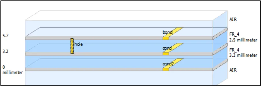
Chapter VI
Design of a Multiband Stacked Microstrip Patch antenna for Satellite
Communications
In this chapter, a Multiband stacked microtsrip patch antenna was designed. The antenna has multiple resonant frequencies that can be utilized to serve satellite communications as well as other communication systems. The main resonant frequency designed at 1.487 GHz, where 25 MHz bandwidth of Circular polarization is achieved. The antenna consists of three conducting surfaces, one serve as a ground plane and the other two as radiating antennas. Moreover, the two conducting surfaces are coupled through two conducting VIAs. In addition, the antenna uses two different feeding techniques which are Microstrip line and VIAs. The designed antenna is easy to model, fabricate, manufacture, and implement on other communication systems and electronics.
59
6.1Design of Simple Microtsrip Patch antenna that radiates at 1.6 GHz
The main aim of this thesis is to develop a microstrip patch antenna that can be utilized in satellite communication. Since mobile and handheld devices antennas’ design has developed over the years, antennas that are used for satellite communications especially with the handheld devices needs to improve. The main improvement to these antennas over the time is converting from monopole antennas to microstrip patch antenna since microstrip patch antennas are smaller, compact and easy to integrate with the handheld devices. However, the same has not been
considered for satellite communications. As a result, the main contribution of the thesis is to develop a microstrip patch antenna that can be used instead of monopole antennas in the
handheld devices for satellite communications. A case study was considered is Thuraya Satellite Communication Company which has a widely spread handheld devices but with monopole antennas. Thuraya is using both 1.5 GHz and 1.6 GHz as center frequencies for Satellite communication Uplink and Downlink respectively. It is worth mentioning that Thuraya considerations is for the study purposes to prove the concept only whereas the same can be extended over the other Applications / Satellite Companies.
60
6.1.1 Simple Antenna Design:
Simple rectangular microstrip patch antenna was considered in the beginning. To design a rectangular microstrip patch antenna, there are five steps that need to be followed as deafened by Balanis in [2]. The five steps are:
Step 1: Calculation of the Width (W):
(3)
Step 2: Calculation of the Effective Dielectric Constant Eeff:
(4)
Step 3: Calculation of the Effective length:
(5)
Step 4: Calculation of the length extension ΔL:
61 Step 5: Calculation of actual length of the patch:
(7)
Where the following parameters are used: 1. f0: Resonance Frequency
2. W: Width of the Patch 3. L: Length of the Patch
4. h: Thickness of the Patch antenna
5. εr: Relative Permittivity of the dielectric substrate
6. c: Speed of light: 3 x 10⁸ m/s2
Therefore, to design a rectangular microtsrip patch antenna, three main parameters needs to be defined which are the dielectric material (the substrate), thickness of the substrate, and the operating frequency of the antenna. The dielectric material that is proposed to be used is FR_4, which is a widely used dielectric material with a relative permittivity Er of 4.6. the main reason for choosing this material is the availability and the wide utilization of this material in microstrip patch antennas.
62
The last parameter to design our antenna is the operating frequency which is chosen to be 1.6 GHz as indicated earlier. By designing our antenna following the five steps of Balanis [2], the Width of the antenna is 55mm and the length of the antenna is 43 mm.
The antenna was designed and constructed using ADS as in Fig.65 and return loss as in Fig.66.
63
Fig.66 Return loss of the simple rectangular antenna
However, this antenna is not square antenna. Therefore, to apply Balanis [2] and the work in [16] in order to obtain circular polarization, the antenna dimensions needs to be modified to be square antenna. It is important to note that, for microstrip patch antennas, theoretical equations applies for the simplest antenna designs like rectangular patch antenna. However, for more complicated designs, the implementations or simulations results define mainly how each design stage affected the antenna behavior. As a result, the antenna dimensions were modified to maintain the same results obtained in the simple antenna; hence the dimensions of the antenna became a square antenna of 45 x 45 mm dimensions.
45 mm x 45 mm antenna was constructed in ADS and simulated to check for the resonant frequency. Fig.67 represents the antenna layout. Fig.68 represents the return loss of the
64
Fig.67 Simplest square antenna
Fig.68 Return Loss of the simplest square antenna Feeding
Point
Resonant Freq. at 1.75
65
This simple square antenna return loss falls around the resonant frequency of our desire which is 1.6 GHz. However, the resonance frequency needs further modifications in order to have better matching. Furthermore, this rectangular antenna is not expected to have a circular polarization. As a result, two main parameters of this antenna need to be modified. The first is the Circular polarization of the antenna. The second thing is matching at the desired resonance frequency.
6.1.2 Circular Polarization and Resonance Frequency Modifications:
From the work in [16], the corner cut to achieve circular polarization is 13 mm with 45 degrees angle. Giving the length or the width is 47.6 mm, then the length of the cut is 13 Cos 47.6 = 9.19 mm. As a principle, if the percentage of the cut is applicable, hypothetically, then for a rectangular antenna with center feed a corner cut of 9.19 / 47.6 = 0.193 or 19.3 % of the sides will result in an antenna that has a circular polarization performance at the center frequency. Applying this principle to our designed antenna of 45 x 45 rectangular antenna to check the possibility to obtain the same results. The corner cut to our antenna is 19.3 % of 45 mm = 8.69 mm. The antenna is constructed as in Fig.69 with the corner cuts calculated earlier. CP of the antenna is better to be obtained after having better matching of the resonant frequency.
66
Fig.69 45 x 45 mm Antenna with corner cuts to achieve circular polarization
One of the simplest ways of enhancing the matching at the resonance frequency of the antenna is to increase the matching between the feeding point and the antenna itself. The feeding line that feeds the antenna has certain impedance. On the other hand the antenna as a complete object has also overall impedance. Matching the antenna impedance with the feeding point impedance decreases the amount of the reflected signals to the feeding point due to the
mismatching of the impedances. Therefore, one of the useful methods to increase the matching between these two ends is using a feeding line which will match the impedance of the two
different ends. ADS gives a simple way to find the details of the feeding line dimensions through the use of the LineCalc tool, as in Fig.70, tool which will calculate the length of the feeding line. This feeding either it is extended to the antenna or it is an inset in the antenna itself.
67
Fig.70 LineCalc tool in ADS to find the length of the Feeding line
68
Fig.71 Proposed with extended feeding line
Fig.72 Antenna with inset matching line
Feeding Line
69
Fig.73 Return loss of antenna in Fig.71
Fig.74 Return loss of antenna in Fig.72
70
polarization if the axial ratio of the radiating element of the antenna is 0 dB. However, for the practical applications 3 dB Axial ratio or below is an acceptable value to consider the antenna is having a circular polarization at a certain frequency. Fig.75 represents the axial ratio of the antenna designed.
Fig.75 Axial Ratio of the simple antenna
From the proceedings, the axial ratio of 3 dB and less is from around 1.53 GHz to 1.555 GHz. Therefore, circular polarization is achieved over this bandwidth of 25 MHz. Moreover, the simple antenna is simulated from 0.5 GHz to 6 GHz as in Fig.76 to check for other resonant frequencies. The results obtained show a good matching of the antenna at 3 GHz and around 5.8 GHz. 0 2 4 6 8 10 12 14
1.48 1.5 1.52 1.54 1.56 1.58 1.6 1.62
Frequency VS Axial Ratio
Series1
71
Fig.76 Return loss of the simple antenna from 0.5 GHz to 6 GHz Three
72
6.2Improving the antenna bandwidth at the resonant frequency:
After finalizing the simple antenna that is chosen for our design, different enhancement techniques were explored and applied to our antenna in order to improve the bandwidth of the simple antenna. The simple antenna designed have a resonant frequency around 1.6 GHz. However, the bandwidth of this resonant frequency is very narrow. Moreover, the circular polarization bandwidth obtained is somehow falling to the left of the resonant frequency. Therefore, in this section the antenna in modified to have a wider bandwidth at the desired resonant frequency. However, the resonant frequency shifts to the left due to this modification to be around 1.48 GHz with a wider bandwidth of around 50 MHz. The modified antenna has three layers of conducting materials, the ground plane and two more conducting patches on top of each other. The middle patch is the same of the simple antenna fed through feeding line. The other patch on top of the simple antenna is being fed through a VIA from the lower patch.
Modified Antenna Design:
Now, different enhancement techniques is explored in order to improve the bandwidth of the simple antenna at the resonant frequency 1.6 GHz . The following presentation represents the major techniques implemented to obtain the desired bandwidth:
6.2.1 Extra layer on top with Electromagnetic coupling:
73
resonant frequency with wider bandwidth. Fig.77 represents the antenna cross section of the added patch and the substrate material which is similar to the material used for the lower antenna substrate. Furthermore, Fig.78 shows the schematic of the antenna with the top layer that
matches the lower antenna “the simple antenna”, but with shrunk dimensions.
Fig.77 Two patch antenna cross section
Fig.78 Schematic of the two patch antenna
Upper patch and second
Substrate
Ground Plane
Upper Substrate
74
The antenna is simulated and the result of the return loss of the antenna is shown in Fig.79. From the return loss, it is obvious that the bandwidth of the antenna shifted to the left towards lower frequencies around 1.48 GHz. The main reason for that shift of the resonant frequency is the upper new patch.
Fig.79 Return loss of the two patch antenna
In addition, the antenna simulated at 1.5 GHz and the surface current of the antenna was obtained as in Fig.80. The main reason of the surface current simulation is to check the coupling between the two patches. Currently, the upper patch is being fed through the electromagnetic coupling between the two patches, which induces a surface current on the upper patch and hence the upper patch radiates the signals. Having a good coupling between the two patch antennas means that the majority of the radiated signals from the lower patch is being transferred to the upper patch and hence radiated from the whole antenna. On the other hand, if there is a poor
New resonant frequency with
75
surface current on the upper patch that means there is high percentage of the signals radiated from the lower patch is being reflected back. Therefore and as It is clearly obvious in Fig.80, there is a very low surface current on the top antenna while there is a good current surface on the lower antenna. Having low surface current on the top antenna, means there is a low
electromagnetic coupling between the upper and the lower antennas. In our goal to enhance the antenna performance, a conducting VIA was added between the two layers to improve the electromagnetic coupling between the two layers.
Fig.80 Surface Current of the electromagnetically coupled two patches Lower patch
with high surface current
76
6.2.2 Extra layer on top with VIA conductor:
Giving that the upper antenna has a relatively very low electromagnetic coupling with the lower antenna, therefore, a conducting VIA is proposed to be between the two conducting layers in order to have better surface current on the top antenna and hence having better matching at the resonant frequency. Fig.81 shows the antenna cross section with the VIA, while Fig.82 show the antenna schematic with the VIA being located at the center of the lower and upper patch.
Fig.81 Antenna cross sections with VIA being added between the two patched
Fig.82 Schematic of the VIA
VIA between the lower and the upper patch Conducting
77
The antenna is simulated and return loss of the antenna with a VIA coupling the two patches in shown in Fig.83. It is obvious from the simulations that there is not huge difference between the two methods. However, there is a better matching when the VIA was used.
Therefore, the VIA is kept and further enhancement was done to the antenna in order to improve its bandwidth.
Fig.83 Return loss of the Antenna with VIA between the two patches 6.2.3 Changing the location of the VIA and the Conductor size:
78
Fig.84 Antenna with Left VIA, and increased VIA conductor size
Fig.85 Antenna with Right VIA, and increased VIA conductor size Right VIA with
increased conducting size
79
Both antennas were simulated for the return loss as in Fig.86, 87 for both left and right VIA respectively. From the simulations it is obvious that the antenna with the conducting VIA to the right is having better matching at the resonant frequency. Moreover, it has a slight