Experimental Observation on Solid-State Reactive Diffusion
between Sn–Ag Alloys and Ni
Misako Nakayama
1, Minho O
2and Masanori Kajihara
2,*1Graduate School, Tokyo Institute of Technology, Yokohama 226–8502, Japan
2Department of Materials Science and Engineering, Tokyo Institute of Technology, Yokohama 226–8502, Japan
The kinetics of the solid-state reactive diffusion between Sn–Ag alloys and pure Ni was experimentally observed to examine effects of addition of Ag into Sn on the growth behavior of compound at the interconnection between the Sn-base solder and the multilayer Au/Ni/Cu conductor during energization heating. In this experiment, sandwich (Sn–Ag)/Ni/(Sn–Ag) diffusion couples with Ag concentrations of y = 0.011–0.033 were prepared by a diffusion bonding technique, and then isothermally annealed at temperatures of T = 453–473 K for various periods up to 3169 h, where y is the mol fraction of Ag. After annealing, an intermetallic layer consisting of Ni3Sn4 was recognized between the Sn–Ag and Ni specimens in the diffusion couple. Here, the concentration of Ag in Ni3Sn4 is negligible. The mean thickness of the intermetallic layer is proportional to a power function of the annealing time, and the exponent of the power function takes values of 0.33–0.43 at T = 453 K and those of 0.54–0.62 at T = 473 K. Thus, the growth of the intermetallic layer is controlled by boundary and volume diffusion at T = 453 K. In contrast, at T = 473 K, interface reaction and interdiffusion contribute to the rate-controlling process of the intermetallic growth. The addition of Ag into Sn accelerates the intermetallic growth within the experimental annealing times. [doi:10.2320/matertrans.M2016409]
(Received November 14, 2016; Accepted January 30, 2017; Published March 10, 2017)
Keywords: reactive diffusion, metallization, solder, conductor, intermetallic compounds
1. Introduction
Various Sn-base alloys are used as Pb-free solders in the
electronics industry.1–8) They are Sn–Ag alloys, Sn–Cu
al-loys, Sn–Ni alal-loys, Sn–Zn alal-loys, etc. Among such Sn-base alloys, the Sn–Ag alloy is one of the most favorable candi-dates of Pb-free solders.9–20) On the other hand, owing to high
electrical conductivity, Cu-base alloys are widely utilized as conductor materials in the electronics industry. When the Cu-base conductor is interconnected with a Sn-Cu-base solder, Cu6Sn5 and Cu3Sn are formed at the interconnection between
the conductor and the solder during soldering and then grad-ually grow during energization heating at solid-state
tempera-tures.21–31) Since the Cu–Sn compounds are brittle and
pos-sess high electrical resistivities, their growth deteriorates the mechanical and electrical properties of the interconnection. To inhibit the formation of the compounds, the Cu-base con-ductor is usually plated with a Ni layer. However, Ni is not sufficiently corrosion resistant. Hence, the Ni layer is plated with a Au or Pd layer to improve corrosion resistance.32–35)
For the multilayer Au/Ni/Cu conductor with a thin Au lay-er, the Au layer quickly dissolves into a molten Sn-base sol-der during solsol-dering, and then the Ni layer is contacted with the solder. As a consequence, the Ni layer is directly reacted with the solder during solid-state energization heating. The solid-state reactive diffusion in the Sn/Ni system was
experi-mentally examined using sandwich Sn/Ni/Sn diffusion
cou-ples prepared by a diffusion bonding technique in a previous study.36) In this experiment, the diffusion couples were
iso-thermally annealed at temperatures of T = 433–473 K. At the interface in the annealed diffusion couple, a layer of Ni3Sn4
was observed at T = 453–473 K, but granular particles of Ni3Sn4 were recognized at T = 433 K. The mean thickness of
the Ni3Sn4 layer is proportional to a power function of the
annealing time. The exponent of the power function is 0.46
and 0.41 at T = 453 and 473 K, respectively. The exponent smaller than 0.5 indicates that the growth of Ni3Sn4 is
con-trolled by boundary and volume diffusion and grain growth occurs in Ni3Sn4. Although the growth of Ni3Sn4 may be
ac-celerated by boundary diffusion, the overall growth rate is smaller for Ni3Sn436) than for Cu6Sn5 and Cu3Sn.23,31)
Conse-quently, the Ni layer works as a barrier against the reactive diffusion at the interconnection between the Sn-base solder
and the multilayer Au/Ni/Cu conductor with a thin Au layer
during solid-state energization heating.
As previously mentioned, the Sn–Ag and Sn–Cu solders are typical Pb-free Sn-base solders. For the Sn–Cu solder, small particles of Cu6Sn5 are dispersed in the Sn matrix. The
dispersion of Cu6Sn5 in the solder may influence the kinetics
of the solid-state reactive diffusion between the Sn matrix and the Ni layer at the interconnection. To examine this influence,
the kinetics of reactive diffusion in the (Sn–Cu)/Ni system
was experimentally observed at temperatures of T = 453–
473 K using sandwich (Sn–Cu)/Ni/(Sn–Cu) diffusion
cou-ples with Cu mol fractions of 0.01–0.03 prepared by a
diffu-sion bonding technique in a previous study.37) According to
the observation, an intermetallic layer consisting of (Cu,Ni)6Sn5 and Ni3Sn4 is formed at the original interface
be-tween the Sn–Cu and Ni specimens in the diffusion couple during annealing. The total thickness of the intermetallic lay-er increases in proportion to a powlay-er function of the anneal-ing time, and the exponent of the power function takes values of 0.37–0.44 at T = 453 K and those of 0.63–0.69 at T = 473 K. Therefore, the growth of the intermetallic layer is con-trolled by boundary and volume diffusion at T = 453 K. On the other hand, at T = 473 K, interface reaction and interdiffu-sion contribute to the rate-controlling process of the interme-tallic growth. The addition of Cu into Sn accelerates the inter-metallic growth within the experimental annealing times. As a consequence, it is concluded that the Cu addition foments the deterioration of the mechanical and electrical properties of the interconnection during energization heating at solid-
*
state temperatures.
In contrast, for the Sn–Ag solder, small particles of Ag3Sn
are distributed in the Sn matrix. Like the Cu6Sn5 particle in
the Sn–Cu solder, the Ag3Sn-particle distribution may
influ-ence the kinetics of the solid-state reactive diffusion at the interconnection for long periods. Unfortunately, however, re-liable information on such influence is rather limited. To ex-amine this influence, the kinetics of reactive diffusion in the
(Sn–Ag)/Ni system was experimentally observed at solid-
state temperatures of T = 453–473 K using sandwich (Sn–
Ag)/Ni/(Sn–Ag) diffusion couples with Ag mol fractions of
0.011–0.033 in the present study. A diffusion bonding tech-nique was used to prepare the diffusion couples in a manner similar to previous studies.31,36,37) The rate-controlling
pro-cess of the solid-state reactive diffusion was discussed on the basis of the experimental result.
2. Experimental
Binary Sn–Ag alloys with Ag concentrations of y = 0.011, 0.022 and 0.033 were obtained as 1 kg commercial ingots, where y is the mol fraction of Ag. Plate specimens with size
of 12 mm × 5 mm × 2 mm were prepared by cold rolling and
spark erosion from the ingots. The plate specimens were iso-thermally heated in an oil bath with silicone oil at 473 K for 2 h, followed by water quenching. The two surfaces with area
of 12 mm × 5 mm of each heated Sn–Ag plate specimen were
mechanically polished on # 800 emery paper. One of the two polished surfaces was again mechanically polished on #
1500–4000 emery papers until depth of 100 μm and then
fin-ished using diamond with diameter of 1 μm.
Sheet specimens with size of 20 mm × 7 mm × 0.2 mm
were cut from a pure Ni commercial sheet with dimensions of
300 mm × 100 mm × 0.2 mm and purity of 99.97% and then
separately annealed in evacuated silica capsules at 1173 K for 2 h, followed by air cooling without breaking the capsules. The annealed sheet specimens were chemically polished in nitrohydrochloric acid for 60 s.
After chemical polishing, a Ni sheet specimen was imme-diately sandwiched between the finished surfaces of two freshly prepared Sn–Ag plate specimens in ethanol by the
technique used in a previous study.31) The sandwich (Sn–
Ag)/Ni/(Sn–Ag) couples were completely dried and then
heat treated for diffusion bonding in the oil bath for 65 h at 453 K and 473 K. After the heat treatment, the diffusion cou-ples were isothermally annealed at 453 K and 473 K for vari-ous times up to 3104 h. The summation of the heat-treating and annealing times at the equivalent temperature is hereafter merely called the annealing time t, and the annealing tem-perature is denoted by T. The chemical composition of the Sn–Ag alloy is described as Sn–yAg. The Sn–0.011Ag, Sn– 0.022Ag and Sn–0.033Ag alloys are designated alloys A1, A2 and A3, respectively, and the diffusion couples with alloys A1, A2 and A3 are called diffusion couples A1, A2 and A3, respectively. Cross-sections of the annealed diffusion couple were mechanically polished using diamond with diameters of 15 μm, 3 μm and 1 μm, and then finished with an OP-S liquid manufactured by Struers Ltd. The microstructure of the cross-section was observed by differential interference con-trast optical microscopy (DICOM). Concentrations of Sn, Ag
and Ni in each phase on the cross-section were measured by electron probe microanalysis (EPMA) using pure Sn, Ag and Ni with purity of 99.99% as standard specimens under the following conditions: the accelerating voltage was 20 kV; the probe current was 5 nA; the analyzing crystal was
polyeth-ylene terephthalate (PET) for Sn–Lα and Ag–Lα and lithium
fluoride (LiF) for Ni–Kα; and the chemical composition was
evaluated by a standard ZAF correction technique.
3. Results and Discussion
3.1 Microstructure
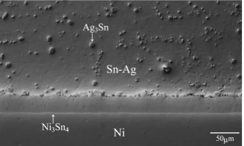
A typical DICOM image for the cross-section of diffusion couple A3 with T = 473 K and t = 560 h (2.016 Ms) is shown in Fig. 1. In this figure, the top and bottom regions are the Sn–Ag and Ni specimens, respectively. For the Sn–Ag speci-men, particles of Ag3Sn are dispersed in the Sn matrix. As can
be seen, a layer with rather uniform thickness is formed at the original interface between the Sn–Ag and Ni specimens. To identify each phase, concentration profiles of Sn, Ag and Ni were determined by EPMA along the direction normal to the original interface. A result for the diffusion couple shown in Fig. 1 is indicated in Fig. 2. In Fig. 2, the ordinate and the abscissa show the mol fraction yi of component i and the dis-tance x measured from an arbitrary origin, respectively, and open circles, rhombuses and squares represent the mol frac-tions ySn, yAg and yNi, respectively. The whole concentration
range is indicated in Fig. 2(a), and the low concentration range of Fig. 2(a) is magnified in Fig. 2(b). As can be seen in Fig. 2(a), the layer consists of Ni3Sn4. On the other hand, in
Fig. 2(b), yNi is typically smaller than 0.006 for the Sn–Ag,
and ySn is smaller than 0.002 for the Ni. Although Ag is
slight-ly soluble in the Ni, yAg is negligible for Ni3Sn4 and the Sn
matrix. Exceptionally larger values of yAg for the Sn–Ag are
attributed to the dispersion of Ag3Sn particles. Such a result
was obtained for all the annealed diffusion couples. Hereaf-ter, the Ni3Sn4 layer is merely called the intermetallic layer. If
we observe the edge of diffusion couple on the cross-section, we can find the location of the original (Sn–Ag)/Ni interface. This observation indicates that the intermetallic layer grows mainly into the Sn–Ag but slightly towards the Ni.
3.2 Growth behavior of intermetallic layer
The schematic morphology of the intermetallic layer on
[image:2.595.308.549.617.761.2]cross-section i is shown in Fig. 3. From the cross-sectional DICOM images, such as that indicated in Fig. 1, the area Ai of the intermetallic layer corresponding to the partial length wi
of the original (Sn–Ag)/Ni interface in Fig. 3 were measured
for cross-section i, and then the sums A and w were obtained by the equations31)
A=
m
i=1
Ai (1a)
and
w=
m
i=1
wi (1b)
from Ai and wi, respectively, where wi = 422 μm and m ≥ 5. Using the values of A and w, the mean thickness l of the inter-metallic layer was evaluated at each annealing time t as fol-lows:31)
l= A
w. (2)
The results of diffusion couples A1, A2 and A3 are plotted as open rhombuses, squares and circles, respectively, in Fig. 4,
Fig. 2 Concentration profiles of Sn, Agand Ni across the intermetallic layer for the diffusion couple shown in Fig. 1: (a) whole concentration range and (b) low concentration range.
Fig. 3 Schematic of morphology for the intermetallic layer on cross-sec-tion i.
[image:3.595.69.270.68.463.2] [image:3.595.324.527.311.705.2]where the ordinate and the abscissa show the logarithms of l and t, respectively. In this figure, open triangles indicate the corresponding results of diffusion couple A0 reported in a
previous study.36) Here, diffusion couple A0 stands for the
Sn/Ni/Sn diffusion couple with y = 0.36) Figure 4(a) and 4(b)
indicates the results for T = 453 and 473 K, respectively. As can be seen in Fig. 4(b), the thickness l monotonically in-creases with increasing annealing time t. Furthermore, the plotted points for each diffusion couple are located well on a straight line. Consequently, l is expressed as a power function of t as follows.
l=k t t0
n
(3)
Here, t0 is unit time, 1 s. It is adopted to make the argument t/
t0 of the power function dimensionless. The proportionality
coefficient k has the same dimension as the thickness l, and the exponent n is dimensionless. The dimensionless argument of the power function is essentially important; otherwise the dimension of k varies depending on the value of n. On the other hand, the open symbols are rather scattered in Fig. 4(a). As mentioned earlier, the diffusion couples were prepared by a diffusion bonding technique. As the bonding temperature decreases, however, it becomes more difficult to realize sound bonding. In the present study, sound bonding was actualized more readily at T = 473 K than at T = 453 K. As a result, the open symbols lie well on the corresponding straight line at
T = 473 K in Fig. 4(b), but they are rather scattered at T = 453 K in Fig. 4(a). From the open symbols plotted in Fig. 4, k and n in eq. (3) were determined by the least-squares method as shown with various straight lines. The determined values are shown in Fig. 4.
Since n varies depending on y, it is rather difficult to find a systematic relationship between k and y. Therefore, to esti-mate the composition dependence of the overall growth rate of the intermetallic layer, the thickness l6 at t = 106 s (1 Ms) is
plotted against y as open squares and circles for T = 453 and 473 K, respectively, with error bars in Fig. 5. Hereafter, the
error bar represents the standard error. For T = 453–473 K, l6
monotonically increases with increasing value of y at y < 0.01 but becomes rather insensitive to y at y > 0.01. For reactive diffusion in binary alloy systems, the growth rate of a com-pound phase is predominantly determined by the interdiffu-sion coefficient of the growing compound phase.38–47) As
pre-viously mentioned, the intermetallic layer consists of Ni3Sn4.
The interdiffusion coefficient D Ni3Sn4 of Ni
3Sn4 may vary
depending on the concentration yNi3Sn4
Ag of Ag in Ni3Sn4. Since yNi3Sn4
Ag is negligible as shown in Fig. 2(b), however, D Ni3Sn4 is rather independent of the value of y. Thus, the dependence of
l6 on y in Fig. 5 cannot be explained by that of D Ni3Sn4 on y.
The result in Fig. 5 will be discussed again later on.
3.3 Rate-controlling process of intermetallic growth
The values of n at T = 453 and 473 K are plotted against y as open circles with error bars in Fig. 6(a) and 6(b), respec-tively. If the layer growth of the intermetallic layer is
con-trolled by volume diffusion, n is equal to 0.5.38–47) On the
other hand, boundary diffusion may govern the layer growth at low temperatures where volume diffusion is frozen out. When the layer growth is controlled by boundary diffusion
Fig. 5 The thickness l6 at t = 106 s versus the mol fraction y of Ag in the Sn–Ag alloy shown as open squares and circles for T = 453 and 473 K, respectively, with error bars. The corresponding results of y = 036) are also represented.
[image:4.595.326.527.355.751.2] [image:4.595.69.273.549.742.2]across the intermetallic layer and grain growth occurs in the intermetallic layer, n becomes smaller than 0.5.48) If the grain
growth slows down, the volume fraction of grain boundaries in the intermetallic layer remains almost constant and hence the effective cross-section for the boundary diffusion hardly varies during annealing. In such a case, n is also equivalent to 0.5, even if the layer growth is purely governed by the bound-ary diffusion. Therefore, there are two possibilities for the rate-controlling process in the case of n = 0.5.
According to the results in Fig. 6, n takes values of 0.33– 0.46 for y = 0–0.033 at T = 453 K and that of 0.41 for y = 0 at
T = 473 K. The values of n smaller than 0.5 indicate that
boundary diffusion as well as volume diffusion controls the layer growth and grain growth takes place in the intermetallic layer. In order to observe experimentally the grain growth, various etchants were used for chemical etching of the inter-metallic layer. However, no appropriate etchant was found in the present study. Nevertheless, n becomes smaller than 0.5 only in the case that boundary diffusion as well as volume diffusion governs the layer growth and grain growth occurs in the intermetallic layer. Such a rate-controlling process is surely guaranteed from a theoretical point of view,48) though
the observation of grain growth was difficult in the present
study. In previous studies,49–55) however, grain growth was
actually recognized for solid-state reactive diffusion between Sn and various metals.
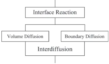
In contrast, n takes values of 0.54–0.62 for y = 0.011–0.033 at T = 473 K. The rate-controlling process of the layer growth is schematically depicted in Fig. 7. If the interface reaction at the moving interface controls the layer growth, n is equivalent to unity.56–64) As mentioned in Section 3.1, the intermetallic
layer grows predominantly into the Sn–Ag specimen. Thus, the values n = 0.54–0.62 indicate that the layer growth is gov-erned by the interface reaction at the migrating Ni3Sn4/(Sn–
Ag) interface and the interdiffusion across the intermetallic layer. Such a mixed rate-controlling process of reactive diffu-sion has been observed for various metal systems. For
in-stance, the reactive diffusion in the (Cu–Sn)/Nb system was
experimentally examined using diffusion couples consisting of Cu–Sn alloys and Nb in previous studies.56–58) In these
ex-periments, the diffusion couple was isothermally annealed at
T = 923–1053 K. During annealing, a single-phase Nb3Sn
layer is formed at the original (Cu–Sn)/Nb interface in the
diffusion couple and grows mainly towards the Nb. Here,
Nb3Sn is one of the most important superconducting
materi-als.
According to the dependence of n on y for T = 453 K in
Fig. 6(a), n is slightly smaller for y = 0.011–0.033 than for y = 0. This implies that the contribution of boundary diffusion to the interdiffusion across the intermetallic layer is greater for
y = 0.011–0.033 than for y = 0. As can be seen in Fig. 1, Ag3Sn
particles on the Ni3Sn4/(Sn–Ag) interface are identifiable, but
each grain in the intermetallic layer is not clearly distinguish-able. If we carefully look at Fig. 1, however, we may
recog-nize that the gathered morphology of the Ni3Sn4/(Sn–Ag)
interface is attributed to the polycrystalline microstructure of
the intermetallic layer.65) From the gathered interface in
Fig. 1, we can roughly estimate the mean grain size d of Ni3Sn4 to be about 4 μm for y = 0.033 at T = 473 K. On the
other hand, d is about 7 μm for y = 0 at T = 473 K according to the corresponding result in a previous study.36) Hence, the
addition of Ag into Sn decreases the value of d, though the solubility of Ag in Ni3Sn4 is negligible as shown in Fig. 2(b).
If the nucleation of Ni3Sn4 at the original (Sn–Ag)/Ni
inter-face is accelerated by the interinter-face segregation of Ag, small values of d are realized by the Ag addition. Consequently, d can be smaller for y = 0.011–0.033 than for y = 0 not only at
T = 473 K but also at T = 453 K. Smaller values of d yield
larger values of the effective interdiffusion coefficient DNi3Sn4 e in the intermetallic layer. As a result, the contribution of boundary diffusion to the interdiffusion will become greater for y = 0.011–0.033 than for y = 0. This may be the reason why the growth rate of the intermetallic layer is greater for
y = 0.011–0.033 than for y = 0 in Fig. 5. Furthermore, the growth rate is greater for T = 473 K than for T = 453 K. If the growth rate exceeds a certain critical value, the interface reac-tion will work as resistance more remarkably, and thus its contribution to the rate-controlling process may become more predominant. As a consequence, n is greater than 0.5 for y = 0.011–0.033 at T = 473 K as indicated in Fig. 6(b).
4. Conclusions
The solid-state reactive diffusion in the (Sn–Ag)/Ni
sys-tem was experimentally observed using the (Sn–Ag)/Ni/
(Sn–Ag) diffusion couples with Ag mol fractions of y = 0.011–0.033. The diffusion bonding technique was used to prepare the diffusion couples. The diffusion couples were iso-thermally annealed in the temperature range of T = 453–473 K for various times up to t = 3169 h. During annealing, the Ni3Sn4 layer is formed at the original (Sn–Ag)/Ni interface in
the diffusion couple, where the concentration of Ag in Ni3Sn4
is negligible. The mean thickness of the Ni3Sn4 layer
increas-es in proportion to a power function of the annealing time. The exponent of the power function takes vales of 0.33–0.43 at T = 453 K and those of 0.54–0.62 at T = 473 K. Therefore, at T = 453 K, the growth of the Ni3Sn4 layer is controlled by
boundary and volume diffusion. In contrast, at T = 473 K, in-terface reaction as well as interdiffusion contributes to the rate-controlling process of the layer growth. The overall growth of the Ni3Sn4 layer is accelerated by the addition of
Ag into Sn.
Acknowledgements
The present study was supported by the Iketani Science and Technology Foundation in Japan. The study was also
[image:5.595.74.262.661.772.2]tially supported by a Grant-in-Aid for Scientific Research from the Ministry of Education, Culture, Sports, Science and Technology of Japan.
REFERENCES
1) J. Glazer: Int. Mater. Rev. 40 (1995) 65–93.
2) M. Abtew and G. Selvaduray: Mater. Sci. Eng. R 27 (2000) 95–141.
3) K. Suganuma: Curr. Opin. Solid State Mater. Sci. 5 (2001) 55–64.
4) H.W. Miao and J.G. Duh: Mater. Chem. Phys. 71 (2001) 255–271.
5) D.R. Frear, J.W. Jang, J.K. Lin and C. Zang: JOM 53 (2001) 28–33.
6) B.L. Young, J.G. Duh and B.S. Chiou: J. Electron. Mater. 30 (2001) 543–553.
7) K. Zeng and K.N. Tu: Mater. Sci. Eng. R 38 (2002) 55–105.
8) K.S. Bae and S.J. Kim: J. Mater. Res. 17 (2003) 743–746.
9) M. McCormack, S. Jin, G.W. Kammlott and H.S. Chen: Appl. Phys. Lett. 63 (1993) 15–17.
10) W. Yang, R.W. Messler, Jr. and L.E. Felton: J. Electron. Mater. 23 (1994) 765–772.
11) S.K. Kang, R.S. Rai and S. Purushothanman: J. Electron. Mater. 25 (1996) 1113–1120.
12) K.W. Moon, W.J. Boettinger, U.R. Kattner, F.S. Biancaniello and C.A. Handwerker: J. Electron. Mater. 29 (2000) 1122–1136.
13) T.M. Korhonen, P. Su, S.J. Hong, M.A. Korhonen and C.Y. Li: J. Elec-tron. Mater. 29 (2000) 1194–1199.
14) T. Hiramori, M. Ito, Y. Tanii, A. Hirose and K.F. Kobayashi: Mater. Trans. 44 (2003) 2375–2383.
15) W.C. Luo, C.E. Ho, J.Y. Tsai, Y.L. Lin and C.R. Kao: Mater. Sci. Eng. A 396 (2005) 385–391.
16) A. Sharif and Y.C. Chan: J. Electron. Mater. 34 (2005) 46–52.
17) G.Y. Jang and J.G. Duh: J. Electron. Mater. 34 (2005) 68–79.
18) F. Gao, T. Takemoto and H. Nishikawa: Mater. Sci. Eng. A 420 (2006) 39–46.
19) N. Dariavach, P. Callahan, J. Liang and R. Fournelle: J. Electron. Ma-ter. 35 (2009) 1581–1592.
20) P. Schmitt, P. Kaiser, C. Savio, M. Tranitz and U. Eitner: Energy Proce-dia 27 (2012) 664–669
21) L. Zakraysek: Welding Res. Suppl. Nov. (1972) 536–541. 22) K.N. Tu: Acta Metall. 21 (1973) 347–354.
23) M. Onishi and H. Fujibuchi: Trans. JIM 16 (1975) 539–547.
24) H.N. Keller: IEEE Trans. Compon. Hybrids Manuf. CHMT-2 (1979) 180–195.
25) H.N. Keller and J.M. Morabito: Surf. Interface Anal. 3 (1981) 16–22.
26) J.O.G. Parent, D.D.L. Chung and I.M. Bernstein: J. Mater. Sci. 23 (1988) 2564–2572.
27) A.J. Sunwoo, J.W. Morris, Jr. and G.K. Lucey, Jr.: Metall. Trans. A 23 (1992) 1323–1332.
28) P.T. Vianco, P.F. Hlava and A.L. Kilgo: J. Electron. Mater. 23 (1994) 583–594.
29) D.R. Frear and P.T. Vianco: Metall. Trans. A 25 (1994) 1509–1523.
30) S. Choi, T.R. Bieler, J.P. Lucas and K.N. Subramanian: J. Electron. Mater. 28 (1999) 1209–1215.
31) T. Takenaka, S. Kano, M. Kajihara, N. Kurokawa and K. Sakamoto:
Mater. Sci. Eng. A 396 (2005) 115–123.
32) C. Wright: IEEE Trans. Parts Hybrids Packag. PHP-13 (1977) 202– 207.
33) H.N. Keller: IEEE Trans. Compon. Hybrids Manuf. CHMT-5 (1982) 408–419.
34) E.I.-B. Hannech and C.R. Hall: Mater. Sci. Technol. 8 (1992) 817–824.
35) G. Ghosh: Acta Mater. 48 (2000) 3719–3738.
36) M. Mita, M. Kajihara, N. Kurokawa and K. Sakamoto: Mater. Sci. Eng. A 403 (2005) 269–275.
37) M. Nakayama and M. Kajihara: Mater. Trans. 56 (2015) 798–802.
38) M. Kajihara: Acta Mater. 52 (2004) 1193–1200.
39) M. Kajihara: Mater. Sci. Eng. A 403 (2005) 234–240.
40) M. Kajihara: Defect Diffusion Forum 249 (2006) 91–96.
41) M. Kajihara: Mater. Trans. 46 (2005) 2142–2149.
42) M. Kajihara: Mater. Trans. 47 (2006) 1480–1484.
43) M. Kajihara and T. Yamashina: J. Mater. Sci. 42 (2007) 2432–2442.
44) M. Kajihara: Mater. Trans. 49 (2008) 715–722.
45) M. Kajihara: J. Mater. Sci. 44 (2009) 2109–2118.
46) M. Kajihara: Mater. Trans. 51 (2010) 1242–1248.
47) M. Kajihara: Mater. Trans. 53 (2012) 1896–1904.
48) A. Furuto and M. Kajihara: Mater. Trans. 49 (2008) 294–303.
49) T. Takenaka, M. Kajihara, N. Kurokawa and K. Sakamoto: Mater. Sci. Eng. A 406 (2005) 134–141.
50) T. Takenaka, S. Kano, M. Kajihara, N. Kurokawa and K. Sakamoto:
Mater. Trans. 46 (2005) 1825–1832.
51) T. Takenaka, M. Kajihara, N. Kurokawa and K. Sakamoto: Mater. Sci. Eng. A 427 (2006) 210–222.
52) T. Sakama and M. Kajihara: J. Alloy. Compd. 475 (2009) 608–613.
53) T. Sakama and M. Kajihara: Mater. Trans. 50 (2009) 266–274.
54) M. Hashiba, W. Shinmei and M. Kajihara: J. Electron. Mater. 41 (2012) 32–43.
55) M. Hashiba, W. Shinmei and M. Kajihara: J. Electron. Mater. 43 (2014) 247–258.
56) Y. Muranishi and M. Kajihara: Mater. Sci. Eng. A 404 (2005) 33–41.
57) T. Hayase and M. Kajihara: Mater. Sci. Eng. A 433 (2006) 83–89.
58) K. Mikami and M. Kajihara: J. Mater. Sci. 42 (2007) 8178–8188.
59) M. Kajihara and Y. Tejima: J. Phys. Conf. Ser. 165 (2009) 012091, 1–4.
60) Y. Tejima, S. Nakamura and M. Kajihara: J. Mater. Sci. 45 (2010) 919– 928.
61) M. O, Y. Takamatsu and M. Kajihara: Mater. Trans. 55 (2014) 1058– 1064.
62) M. Hashiba, K. Masui and M. Kajihara: Mater. Trans. 56 (2015) 30–39.
63) Y. Yamamoto and M. Kajihara: Mater. Trans. 42 (2001) 1763–1770.
64) Y. Yamamoto and M. Kajihara: J. Electron. Mater. 37 (2008) 1710– 1720.