Kinetics of Solid-State Reactive Diffusion in the (Pd
Cr)
/
Sn System
Masaki Hashiba
+1, Koji Masui
+1and Masanori Kajihara
+2Department of Materials Science and Engineering, Tokyo Institute of Technology, Yokohama 226-8502, Japan
The growth of compounds during energization heating at the interconnection between a Sn-based solder and a multilayer Pd/Ni/Cu conductor may be inhibited by alloying of Pd with Cr. To examine such influence of Cr on the compound growth, the kinetics of solid-state reactive diffusion in the (PdCr)/Sn system was experimentally determined in the present study. Experiments were conducted using Sn/(Pd Cr)/Sn diffusion couples with Cr mol fractions ofy=0.110, 0.215 and 0.323 which were prepared by a diffusion bonding technique. The diffusion couples were isothermally annealed in the temperature range ofT=433473 K for various times up tot=360 h. During annealing, a compound layer consisting of different matrices and lamellar phases is formed at the original (PdCr)/Sn interface in the diffusion couple. From the PdCr side to the Sn side in the compound layer, the matrices are PdSn2, PdSn3and PdSn4, and the lamellar phases are (Cr0.9Pd0.1)3Sn,
(Cr0.95Pd0.05)2Sn, (Cr0.9Pd0.1)Sn and CrSn2. The total thickness of the compound layer is proportional to a power function of the annealing time.
The exponentnof the power function is rather close to 0.5 independent ofyatT=453473 K. AtT=433 K, however,n¼0:5fory=0 0.110, butn=0.70.8 fory=0.2150.323. Thus, the overall compound growth is controlled by volume diffusion fory=00.323 atT=453 473 K and fory=00.110 atT=433 K. On the other hand, fory=0.2150.323 atT=433 K, the interface reaction at the moving interface contributes to the rate-controlling process. The overall growth rate of the compound layer is insensitive toyat y<ycbut monotonically
decreases with increasing value ofyaty>yc, whereyc=0.1 and 0.2 atT=433453 K and 473 K, respectively. Consequently, the compound
growth is actually decelerated by the addition of Cr withy>0.2 into Pd in the multilayer Pd/Ni/Cu conductor. [doi:10.2320/matertrans.M2014202]
(Received May 30, 2014; Accepted October 14, 2014; Published December 5, 2014)
Keywords: metallization, solder, conductor, intermetallics
1. Introduction
Copper-based alloys are widely used as conductor materials in the electronics industry due to high electrical conductivity. If the Cu-based conductor is interconnected using a Sn-based solder, Cu6Sn5and Cu3Sn are formed at the
interconnection between the conductor and the solder during soldering and then gradually grow during energization heating at solid-state temperatures.111) Since the CuSn
compounds are brittle and possess high electrical resistivities, their growth deteriorates the mechanical and electrical properties of the interconnection. To suppress CuSn compound formation, the Cu-based conductor is generally plated with a Ni layer. However, Ni is not sufficiently corrosion resistant. Thus, the Ni layer is plated with a Au or Pd layer to improve corrosion resistance.1215)
The reactive diffusion in the Pd/Sn system was exper-imentally examined at solid-state temperatures using Sn/Pd/ Sn diffusion couples prepared by a diffusion bonding technique in a previous study.16) In this experiment, the
diffusion couples were isothermally annealed at temperatures of T=433473 K. At the Pd/Sn interface in the diffusion couple, PdSn4, PdSn3 and PdSn2 layers are formed at
T=433 K, but only PdSn4 and PdSn3 layers are produced
atT=453 K and 473 K. In this case, the total thickness of the compound layers is proportional to the square root of the annealing time. Such a relationship is called the parabolic relationship. Furthermore, grain growth occurs in the compound layers. As a consequence, the layer growth is controlled by volume diffusion.17) At T=433473 K, however, the overall growth rate of the compound layers is one order of magnitude greater for the reactive diffusion in the Pd/Sn system16) than for that in the Cu/Sn system.11)
Hence, the Pd layer of the multilayer Pd/Ni/Cu conductor accelerates the deterioration of the interconnection during solid-state energization heating.
The effect of Ag on the solid-state reactive diffusion in the Pd/Sn system was experimentally examined in previous studies.18,19)In these experiments, Sn/(PdAg)/Sn diffusion
couples with Ag concentrations of y=0.250.75 were isothermally annealed atT=433473 K, where ystands for the mol fraction of Ag. As toy=0.250.50,18)a PdSn
4layer
dispersed withfine Ag3Sn particles is predominantly formed
at the (PdAg)/Sn interface in the diffusion couple during annealing. On the other hand, for y=0.75,19) a compound layer composed of PdSn4and Ag3Sn lamellae is produced at
the interface. Like the Pd/Sn system, the parabolic relation-ship holds between the thickness of the compound layer and the annealing time also in the (PdAg)/Sn system. Here, the notation (AB)/C means that reactive diffusion occurs between a binary AB alloy and a pure C metal. As the Ag concentrationyincreases, the parabolic coefficient decreases slightly aty<0.5 but remarkably aty>0.5. Therefore, the growth of compounds at the interconnection between the Sn-based solder and the multilayer Pd/Ni/Cu conductor is effectively inhibited by addition of Ag withy>0.5 into Pd. According to a recent phase diagram in the binary PdCr system,20) the solubility of Cr in Pd reaches to y=0.5 at
1588 K. Here, y represents the mol fraction of Cr. The melting temperatureTmis 2136 K and 1828 K for Cr and Pd,
respectively, and henceTmis much higher for Cr than for Pd.
Therefore, we may intuitively expect that alloying of Pd with Cr decelerates the interdiffusion between Pd and Sn and thus inhibits the formation of the PdSn compounds at solid-state temperatures. Unfortunately, however, no reliable informa-tion is available for effects of Cr on the compound formainforma-tion. In the present study, the influence of Cr on the solid-state reactive diffusion between Pd and Sn was experimentally examined using Sn/(PdCr)/Sn diffusion couples with Cr
+1Graduate Student, Tokyo Institute of Technology
+2Corresponding author, E-mail: kajihara@materia.titech.ac.jp
concentrations of y=0.10.3 in the temperature range of 433473 K. The rate-controlling process of the reactive diffusion was discussed on the basis of the experimental result.
2. Experimental
Plate specimens of pure Sn with a size of 12 mm© 5 mm©2 mm were prepared by cold rolling and spark erosion from a commercial 1 kg rectangular ingot of pure Sn with a purity of 99.99%. The cold-rolled plate specimens were separately annealed in evacuated silica capsules at 473 K for 2 h, followed by air cooling without breaking the capsules. The annealed Sn plate specimens were chemically polished in an etchant consisting of 20 vol% of nitric acid, 20 vol%of hydrochloric acid and 60 vol%of distilled water. The two surfaces with an area of 12 mm©5 mm of each Sn plate specimen were mechanically polished on # 800 emery paper. One of the two polished surfaces was again mechanically polished on#15004000 emery papers until a depth of 100 µm, and then finished using diamond with a diameter of 1 µm.
Binary PdCr alloys with Cr mol fractions of y=0.110, 0.215, 0.323 and 0.336 were made as 20 g button ingots by argon arc melting from pure Pd and Cr with purities of 99.9 and 99.99%, respectively. Plate specimens with dimensions of 15 mm©7 mm©3 mm were cut from the button ingot, and then separately homogenized in evacuated silica capsules at 1173 K for 336 h, followed by air cooling without breaking the capsules. Sheet specimens with a size of 12 mm© 5 mm©0.2 mm were prepared by cold rolling and spark erosion from the homogenized plate specimen. Each sheet specimen was annealed in an evacuated silica capsule at 1173 K for 2 h, followed by water quenching without breaking the capsule. The annealed sheet specimen was chemically polished in nitrohydrochloric acid for 60 s.
After chemical polishing, a PdCr sheet specimen was immediately sandwiched between the finished surfaces of two freshly prepared Sn plate specimens in ethanol by the technique used in a previous study.18)Sandwich Sn/(PdCr)/ Sn couples were entirely dried, and then heat treated for diffusion bonding in an oil bath with silicone oil at temperatures of 433 K, 453 K and 473 K for 3 h, 0.75 h and 0.5 h, respectively. After the heat treatment, the diffusion couples were isothermally annealed in this temperature range for various times up to 357 h. The summation of the heat-treating and annealing times is hereafter merely called the annealing timet, and the annealing temperature is denoted by T. The chemical composition of the PdCr alloy is described as PdyCr, where yis the mol fraction of Cr as mentioned earlier. The Pd0.110Cr, Pd0.215Cr, Pd0.323Cr and Pd 0.336Cr alloys are designated alloys C1, C2, C3 and C4, respectively, and the diffusion couples with alloys C1, C2, C3 and C4 are denominated diffusion couples C1, C2, C3 and C4, respectively. As to diffusion couple C4, isothermal annealing was extended to t=2100 h at T=433473 K. Cross-sections of the annealed diffusion couple were mechanically polished using diamond with diameters of 15, 3 and 1 µm, and then finished with an OP-S liquid manufactured by Struers Ltd. The microstructure of the
cross-section was observed by differential interference contrast optical microscopy (DICOM) and scanning electron mi-croscopy (SEM). A backscattered electron image (BEI) technique was preferably used in the SEM observation. Concentrations of Sn, Pd and Cr in each phase on the cross-section were measured by electron probe microanalysis (EPMA). Diffusion couples C1C3 were used mainly for the kinetic observation, and diffusion couple C4 was utilized only for the EPMA measurement.
3. Results and Discussion
3.1 Microstructure
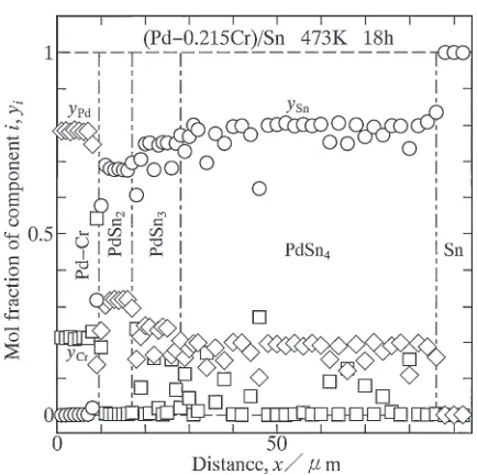
Typical cross-sectional DICOM photographs of diffusion couple C2 annealed at T=473 K are shown in Fig. 1. Figure 1(a) and 1(b) indicates the DICOM photographs of t=9 h (3.24©104s) and t=18 h (6.48©104s), respec-tively. In these photographs, the top region is the Sn specimen, and the bottom region is the PdCr alloy. Here, alloys C1C4 possess the single-phase microstructure with the face-centered cubic (fcc) crystal structure. As can be seen in Fig. 1, a compound layer composed of matrices with different grain sizes and lamellar phases is produced between the Sn and the PdCr alloy. If we observe the edge of diffusion couple on the cross-section, we canfind the location of the original (PdCr)/Sn interface. This observation indicates that the compound layer grows mainly into the Sn but slightly towards the PdCr alloy. To identify each phase, concentration profiles of Sn, Pd and Cr across the compound layer were determined by EPMA along the direction normal to the original (PdCr)/Sn interface. A result of the diffusion couple in Fig. 1(b) is indicated in Fig. 2. In this figure, the ordinate and the abscissa show the mol fraction yi of
component i and the distance xmeasured from an arbitrary origin, respectively, and open circles, rhombuses and squares represent the mol fractionsySn,yPd andyCr, respectively. As
can be seen, the matrices are PdSn2, PdSn3 and PdSn4from
the PdCr side to the Sn side, and the thickness is much smaller for PdSn2 and PdSn3 than for PdSn4. Comparing
Fig. 1(b) with Fig. 2, the fine-grained contrast may be
Fig. 1 Cross-sectional DICOM photographs of the compound layer in diffusion couple C2 annealed atT=473 K for (a)t=9 h (3.24©104s)
[image:2.595.313.541.69.248.2]recognized for PdSn2but not for PdSn3and PdSn4. Thus, in
Fig. 1(b), the interface is distinguishable between PdSn2and
PdSn3but not between PdSn3and PdSn4. Since the thickness
of the compound layer is smaller for Fig. 1(a) than for Fig. 1(b), however, PdSn2is invisible in Fig. 1(a). Although
the concentration of Cr is much larger for the lamellar phases than for the matrices, the thicknesses of the lamellar phases in diffusion couples C1C3 were not sufficiently large
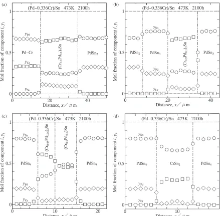
com-pared with the spatial resolution of EPMA. Consequently, unlike the matrices, the chemical compositions of the lamellar phases could not be reliably determined by EPMA. Cross-sectional BEI photographs of diffusion couple C4 with T=473 K andt=2100 h (7.56©106s) are shown in Fig. 3. In Fig. 3(a), the top and bottom regions are the Sn and the PdCr alloy, respectively. As can be seen, the compound layer with a thickness of about 500 µm is produced between the Sn and the PdCr alloy. The lower, middle and upper parts of the compound layer are magnified in Fig. 3(b), 3(c) and 3(d), respectively. At each part, concentration profiles of Sn, Pd and Cr across each second phase were determined by EPMA along the direction normal to the original (PdCr)/Sn interface. Results are shown in Fig. 4. As indicated in Fig. 3(a), a dark layer with a rather uniform thickness is formed between the PdCr alloy and PdSn2. The
concen-tration profiles across this dark layer are shown in Fig. 4(a). According to Fig. 4(a), the dark layer is (Cr0.9Pd0.1)3Sn. On
the other hand, the result in Fig. 4(b) corresponds to the region in Fig. 3(b), and those in Fig. 4(c) and 4(d) correlate to the medium and upper regions in Fig. 3(c), respectively. Figures 3(b) and 4(b) show that (Cr0.9Pd0.1)3Sn is also
distributed as coarse flakes in PdSn3. Since the fine-grained
contrast is rather discerned for PdSn2but not for PdSn3and
PdSn4 in Fig. 3(b), the PdSn2/PdSn3 interface is slightly
distinguishable in this figure. In contrast, thin flakes composed of darker and brighter phases are recognized in Fig. 3(c). Furthermore, the darker phase is surrounded by the brighter phase. Figure 4(c) indicates that the darker and brighter phases are (Cr0.95Pd0.05)2Sn and (Cr0.9Pd0.1)Sn, Fig. 2 Concentration profiles of Sn, Pd and Cr across the compound layer
in diffusion couple C2 shown in Fig. 1(b).
Fig. 3 Cross-sectional BEI photographs of the compound layer in diffusion couple C4 withT=473 K andt=2100 h (7.56©106s):
[image:3.595.61.278.65.281.2] [image:3.595.100.496.457.761.2]respectively, and the matrix is PdSn4. For the medium region
in Fig. 3(c), however, the thickness of (Cr0.9Pd0.1)Sn is not
large enough to conduct the EPMA measurement reliably. Thus, the result in Fig. 4(c) actually corresponds to a different region of the diffusion couple in Fig. 3. On the other hand, a ratherfine lamellar microstructure is observed in Fig. 3(d). Figure 4(d) represents that the matrix and the second phase in the fine lamellar microstructure are PdSn4
and CrSn2, respectively.
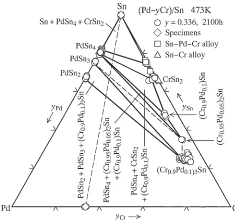
The experimental points in Fig. 4 are plotted as a diffusion path with open circles in a composition triangle of the ternary SnPdCr system in Fig. 5. According to Fig. 4(a) and 4(b), (Cr0.9Pd0.1)3Sn is directly contacted with both PdSn2 and
PdSn3. This implies that the three-phase equilibrium of
PdSn2+PdSn3+(Cr0.9Pd0.1)3Sn exists in this ternary
sys-tem. On the other hand, as indicated in Fig. 4(c) and 4(d), (Cr0.95Pd0.05)2Sn, (Cr0.9Pd0.1)Sn and CrSn2 are distributed
in PdSn4. This means that there appear the three-phase
equilibrium of PdSn4+(Cr0.95Pd0.05)2Sn+(Cr0.9Pd0.1)Sn
and that of PdSn4+(Cr0.9Pd0.1)Sn+CrSn2. As reported in
previous studies, at T=433473 K, the three-phase equi-librium of Sn+PdSn4+CrSn2exists in the ternary SnPd
Cr system,21) and the two-phase equilibrium of Sn+CrSn 2
appears in the binary SnCr system.22) The experimental
compositions of these two-phase and three-phase equilibria are shown as open triangles and squares, respectively, in Fig. 5. Although the solubility of Pd in CrSn2 is small, the
solubility range of CrSn2is slightly extended to the Sn-rich
side by addition of Pd into CrSn2. The same phase
relationships as Fig. 5 were observed also atT=433 K and 453 K. Since the volume fraction of each Cr-rich compound on the cross-section is very small even for diffusion couple C4 with t=2100 h (7.56©106s), however, the crystal structures of the Cr-rich compounds could not be determined by an X-ray diffraction technique.
As shown in Fig. 3, the compound layer with periodic lamellar microstructure is formed owing to the reactive diffusion in the (PdCr)/Sn system at T=433473 K. This
(a) (b)
(c) (d)
[image:4.595.79.518.67.498.2]type of compound formation is usually called a Liesegang phenomenon. Originally, Liesegang found periodic precip-itation of a compound in a solvent.23) On the other hand, a
solid-state Liesegang phenomenon was observed by Osinski et al. for the reactive diffusion in the (FeSi)/Zn system at T=668 K.24)In a previous study,22)a solid-state Liesegang
phenomenon was recognized also for the reactive diffusion in the (NiCr)/Sn system atT=453473 K. The compound formation due to a solid-state Liesegang phenomenon can be explained by a geometrical model reported in a previous study.22)
As mentioned in Section 1, the solid-state reactive diffusion in the Pd/Sn system was experimentally observed using the Sn/Pd/Sn diffusion couple in a previous study.16) Hereafter, the Sn/Pd/Sn diffusion couple is called diffusion couple C0. In diffusion couple C0,16)PdSn4, PdSn3and PdSn2
were observed at T=433 K, but only PdSn4 and PdSn3
were discerned at T=453473 K. On the other hand, in diffusion couples C1C4, PdSn2as well as PdSn4and PdSn3
was clearly recognized atT=433473 K. Hence, the phase stability and the relative growth rate among PdSn4, PdSn3and
PdSn2vary depending on the chemical composition of the Pd
Cr alloy in the Sn/(PdCr)/Sn diffusion couple, though the solubilities of Cr in PdSn4, PdSn3and PdSn2are negligible as
mentioned earlier. In the binary PdSn system,20)ten PdSn compounds with different stoichiometries appear as stable phases at T=433473 K. Of the ten compounds, however, only PdSn4, PdSn3 and PdSn2 were clearly recognized in
diffusion couples C1C4. Therefore, the phase equilibria among the other seven PdSn compounds and the Cr-rich compounds were not determined in the present study.
3.2 Growth behavior of intermetallic layer
As previously mentioned, various compounds are pro-duced in diffusion couples C1C4. The chemical
composi-tion of each compound was reliably determined by EPMA for diffusion couple C4 but not for diffusion couples C1C3. Although the PdSn2/PdSn3 interface is distinguishable in
DICOM photographs, PdSn2 is invisible due to small
thicknesses at short annealing times. Hence, for the kinetic observation using diffusion couples C1C3, only the overall layer growth was examined experimentally. However, the thickness is much greater for PdSn4 than for PdSn2 and
PdSn3, and the volume fraction is much smaller for the
second phases than for PdSn4. As a consequence, the layer
growth of PdSn4 predominantly governs the overall layer
growth. Hereafter, the layer consisting of various compounds is merely called the intermetallic layer. The schematic morphology of the intermetallic layer on cross-section i is shown in Fig. 6. From DICOM photographs such as that shown in Fig. 1, the area Ai of the intermetallic layer
corresponding to the partial lengthwiof the original (PdCr)/
Sn interface in Fig. 6 was measured on each cross-section, and then the sumsAandwwere obtained as18)
A¼Xm
i¼1
Ai (1a)
and
w¼Xm
i¼1
wi (1b)
fromAiand wi, respectively, wherem²5. Using the values
ofAandw, the total thicknesslof the intermetallic layer was evaluated at each annealing time tby the equation18)
l¼Aw: ð2Þ
Here,wandAare the total length parallel to the original (Pd Cr)/Sn interface and the total area of the intermetallic layer, respectively, on the cross-section. The results of diffusion couples C0,16)C1, C2 and C3 atT=433473 K are plotted as open circles, triangles, rhombuses and squares, respec-tively, in Fig. 7(a)(c). According to Fig. 3(a), a very thin crack is observed along the PdSn4/Sn interface in diffusion
couple C4. This thin crack may be formed by aggregation of Kirkendall voids during extended annealing. On the other
Fig. 6 Schematic of the morphology of the intermetallic layer for cross-sectioni.
Fig. 5 Diffusion path for the concentration profiles shown in Fig. 4. The experimental compositions for the three-phase equilibrium of Sn+ PdSn4+CrSn2 in the ternary SnPdCr system21) and the two-phase
equilibrium of Sn+CrSn2 in the binary SnCr system22) are also
[image:5.595.325.516.67.252.2] [image:5.595.48.283.69.289.2]hand, as indicated in Fig. 1, such a crack was not recognized for diffusion couples C0C3 within the experimental annealing times. Since the values oflmeasured for diffusion
couple C4 are considerably scattered due to the crack formation, only the results of diffusion couples C0C3 are included in Fig. 7. In thisfigure, the ordinate and the abscissa show the logarithms oflandt, respectively. As can be seen, the thickness l monotonically increases with increasing annealing time t. Furthermore, the plotted points of each diffusion couple are located well on a straight line. Consequently, l is expressed as a power function of t as follows.
l¼k tt 0
n
ð3Þ
Here, t0is unit time, 1 s. It is adopted to make the argument
t/t0of the power function dimensionless. The proportionality
coefficientkhas the same dimension as the thicknessl, and the exponent n is dimensionless. From the points plotted in Fig. 7,kandnwere determined by the least-squares method as indicated with various straight lines. The determined values are shown in Fig. 7. Sincenvaries depending ony, it is rather difficult tofind a systematic relationship betweenk andy. Therefore, to estimate the composition dependence of the overall growth rate of the intermetallic layer, the thickness l5att=105s is plotted againstyas open rhombuses, squares
and circles forT=433 K, 453 K and 473 K, respectively, in Fig. 8. At T=433453 K, l5 is rather insensitive to y at
y<0.1 but monotonically decreases with increasing value of y at y>0.1. On the other hand, at T=473 K, l5 remains
almost constant independent of y at y<0.2 but gradually decreases with increasing value ofyaty>0.2. As previously mentioned, the intermetallic layer consists of the PdSn compounds dispersed with the lamellar Cr-rich compounds. In order for the intermetallic layer to grow during annealing, the interdiffusion among the constituent components should occur across the Cr-rich compounds as well as the PdSn compounds. The volume fractionfof the Cr-rich compounds in the intermetallic layer increases with increasing value ofy. Hence, the increase infcauses the decrease inl5. This implies (a)
(b)
(c)
Fig. 7 The total thicknesslof the intermetallic layer versus the annealing timetfor diffusion couples C0,16)C1, C2 and C3 shown as open circles,
triangles, rhombuses and squares, respectively, at (a)T=433 K, (b)T=
453 K and (c)T=473 K.
Fig. 8 The thicknessl5att=105s versus the mol fractionyof Cr in the
[image:6.595.60.276.62.696.2] [image:6.595.316.539.68.274.2]that the interdiffusion is more sluggish for the Cr-rich compounds than for the PdSn compounds. Furthermore, the dependencies of l5 on y and T in Fig. 8 indicate that the
difference of the interdiffusion between the Cr-rich com-pounds and the PdSn compounds increases with decreasing annealing temperature. Consequently, it is concluded that the Cr-rich compounds work as effective diffusion barriers against the growth of the intermetallic layer aty>0.2.
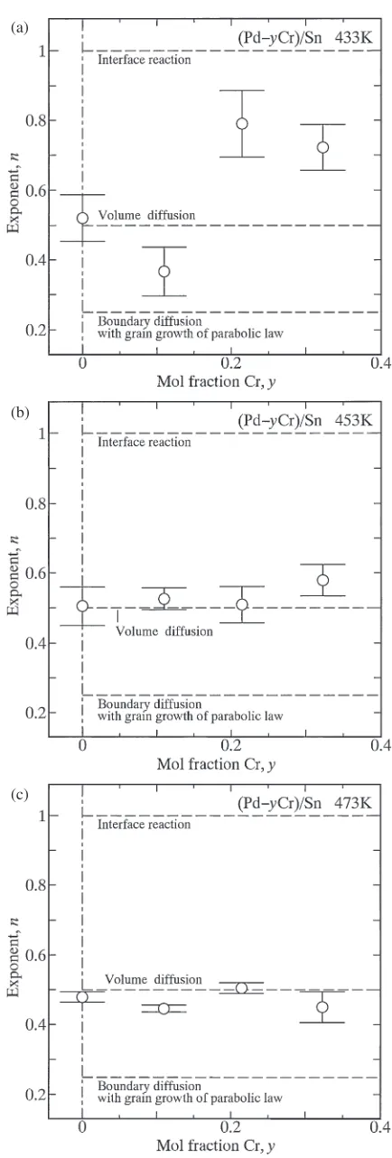
3.3 Rate-controlling process of intermetallic growth The values ofnatT=433 K, 453 K and 473 K are plotted againstyas open circles with error bars in Fig. 9(a), 9(b) and 9(c), respectively. The result in Fig. 9 is represented in a different manner in Fig. 10. In this figure, the ordinate and the abscissa show n and T, respectively, and open circles, triangles, rhombuses and squares indicate the results of y=0,16) 0.110, 0.215 and 0.323, respectively. If the layer
growth of the intermetallic layer is controlled by volume diffusion,nis equal to 0.5.2532)On the other hand, boundary
diffusion may govern the layer growth at low temperatures where volume diffusion is frozen out. When the layer growth is controlled by boundary diffusion across the intermetallic layer and grain growth occurs in the intermetallic layer, n becomes smaller than 0.5.17)However,nis equal to 0.5 even for the layer growth controlled by boundary diffusion unless grain growth takes place.17) Consequently, in the case of n=0.5, there are two possibilities for the rate-controlling process. In such a case, the rate-controlling process cannot be conclusively determined only from the value of n. To estimate the rate-controlling process for the layer growth, the grain growth in the intermetallic layer was experimentally examined for y=0 in a previous study.16) This experiment
indicates that the grain growth actually occurs at T=433 473 K. On the other hand, grain growth in the (PdNi)/Sn system was experimentally observed in a previous study.33) Also in the (PdNi)/Sn system, like the (PdCr)/Sn system, PdSn4, PdSn3and PdSn2are formed atT=433473 K due to
reactive diffusion. In the PdSn compounds, however, the solubility is much greater for Ni than for Cr.33) The grain growth of the intermetallic layer may be decelerated by addition of a solute. Nevertheless, the dissolution of Ni in the PdSn compounds hardly affects the kinetics of grain growth.33) As a result, we may consider that grain growth
takes place also in the (PdCr)/Sn system. Thus, the value n=0.5 guarantees that the layer growth is controlled by volume diffusion. According to Fig. 9, n is close to 0.5 independent of y atT=453473 K and for y=00.110 at T=433 K. Consequently, it is concluded that the layer growth is mostly controlled by volume diffusion under these experimental conditions.
On the other hand, n takes values of 0.7900.722 for y=0.2150.323, respectively, atT=433 K. If the interface reaction at the moving interface governs the layer growth,n is equivalent to unity.3441)As mentioned in Section 3.1, the intermetallic layer grows mainly into the Sn. Thus, the values n=0.7900.722 indicate that the layer growth is controlled by the interface reaction at the PdSn4/Sn interface as well as
the volume diffusion across the intermetallic layer. Such a mixed rate-controlling process of reactive diffusion has been observed for various alloy systems. For instance, the reactive
diffusion in the (CuSn)/Nb system was experimentally examined using diffusion couples consisting of CuSn alloys and Nb in previous studies.3436) In these experiments, the
(a)
(b)
(c)
[image:7.595.317.534.62.703.2]diffusion couple was isothermally annealed at T=923 1053 K. During annealing, a single-phase Nb3Sn layer is
formed at the original (CuSn)/Nb interface in the diffusion couple, and grows mainly towards the Nb. Here, Nb3Sn is
one of the most important superconducting materials. Like the (PdCr)/Sn and (PdNi)/Sn systems, eq. (3) holds between the thicknesslof the Nb3Sn layer and the annealing
time t. The exponent n in eq. (3) is plotted against the annealing temperature T in Fig. 11. In this figure, open triangles, squares and circles show the results of the Cu 8.3Sn,34)Cu8.1Sn0.3Ti35)and Cu9.3Sn0.3Ti36)diffusion
couples, respectively, where the concentrations of Sn and Ti are measured in atomic percent. Since the superconducting properties of Nb3Sn are improved by addition of Ti into the
CuSn alloy, the CuSn alloy contains 0.3 at%of Ti for the latter two diffusion couples. As can be seen in Fig. 11,n is rather close to unity atT=923 K. AsTincreases, however,n gradually decreases, and then reaches to intermediate values of 0.70.8 at T=1053 K. This means that the interface reaction at the Nb3Sn/Nb interface predominantly controls
the growth of the Nb3Sn layer at the lower annealing
temperatures and the volume diffusion across the Nb3Sn layer
contributes to the rate-controlling process at the higher annealing temperatures. Hence, the contribution of volume diffusion increases with increasing annealing temperature. As shown in Fig. 10, such temperature dependence of the rate-controlling process is realized also fory=0.2150.323 in the (PdCr)/Sn system.
For the volume-diffusion rate-controlling process, n is equal to 0.5 as mentioned earlier. In this case, eq. (3) may be rewritten by the following formula.
l2¼Kt¼k2
t0t ð4Þ
Equation (4) is another expression of the parabolic relation-ship. Here, the parabolic coefficient K has a dimension of area per unit time. As previously mentioned,nis close to 0.5 except y=0.2150.323 at T=433 K. Thus, excluding this
exception,Kwas evaluated from the open symbols in Fig. 7 by the least-squares method. The evaluated values ofK are plotted against the annealing temperature Tas various open symbols with error bars in Fig. 12. In thisfigure, the ordinate shows the logarithm of K, and the abscissa indicates the reciprocal of T. Open circles, triangles, rhombuses and squares represent the results of y=0,16) 0.110, 0.215 and 0.323, respectively. For y=00.110, the plotted points are located well on each straight line. Thus, the temperature dependence of Kis expressed by the equation
K¼K0exp QRTK
[image:8.595.315.539.66.283.2]
; ð5Þ
Fig. 10 The exponentnversus the annealing temperatureTfory=0,16)
[image:8.595.59.280.67.282.2]0.110, 0.215 and 0.323 shown as open circles, triangles, rhombuses and squares, respectively.
Fig. 11 The exponentnversus the annealing temperatureTfor the reactive diffusion in the (CuSn)/Nb system. The results of the Cu8.3Sn,34)Cu
8.1Sn0.3Ti35) and Cu9.3Sn0.3Ti36) diffusion couples are shown as
open triangles, squares and circles, respectively.
Fig. 12 The logarithm of the parabolic coefficientKversus the reciprocal of the annealing temperatureTfory=0,16)0.110, 0.215 and 0.323 shown
[image:8.595.317.537.350.553.2]where K0 is the pre-exponential factor, QK is the activation
enthalpy, andRis the gas constant. From the open circles and triangles in Fig. 12,K0 andQKwere evaluated by the
least-squares method fory=0 and 0.110 as shown with solid and dashed lines, respectively. The evaluation gives QK=213
255 kJ/mol fory=00.110, respectively. Although the value QK=255 kJ/mol for y=0.110 is slightly greater than that
QK=213 kJ/mol fory=0,Ktakes similar values fory=0
0.110 at T=433473 K. As a consequence, it is concluded that K hardly varies depending on y within y=00.110 at T=433473 K. Since the exception was excluded as mentioned above, there are merely two plotted points for y=0.2150.323 in Fig. 12. If the two plotted points are interconnected with each other, QK=490418 kJ/mol are
obtained for y=0.2150.323, respectively. Although the evaluation ofQKis less reliable fory=0.2150.323 than for
y=00.110,QKis almost twice greater fory=0.2150.323
than for y=00.110. If the interdiffusion coefficients of all the phases in the diffusion couple are known,Kis estimated by an appropriate mathematical model.2532)In such a case, QKis related to the activation enthalpies of the interdiffusion
coefficients. Unfortunately, however, reliable information is not available even for the self-diffusion coefficient of each component in the Cr-rich compounds and the PdSn compounds. Nevertheless, the volume fraction of each Cr-rich compound should monotonically increase with increas-ing value of y. Therefore, the large values of QK for
y=0.2150.323 imply that the activation enthalpy of the interdiffusion coefficient is much greater for the Cr-rich compounds than for the PdSn compounds.
4. Conclusions
The kinetics of the solid-state reactive diffusion in the (PdCr)/Sn system was experimentally examined using the Sn/(PdCr)/Sn diffusion couples with Cr mol fractions of y=0.110, 0.215 and 0.323. The diffusion couples were isothermally annealed at temperatures ofT=433473 K for various periods up to t=360 h. At the original (PdCr)/Sn interface in the diffusion couple, a compound layer composed of different matrices and lamellar phases is produced due to annealing. The chemical composition of each phase in the compound layer was measured by electron probe micro-analysis (EPMA) using the diffusion couples withy=0.336 annealed for t=2100 h at T=433473 K. The EPMA measurement indicates that the matrices are PdSn2, PdSn3
and PdSn4 from the PdCr side to the Sn side. The
(Cr0.9Pd0.1)3Sn phase is formed as a rather uniform layer at
the (PdCr)/PdSn2 interface and as coarse flakes in PdSn3.
On the other hand, PdSn4 is directly contacted with the
(Cr0.95Pd0.05)2Sn, (Cr0.9Pd0.1)Sn, CrSn2and Sn phases. Thus,
the following three-phase equilibria appear at T=433 473 K in the ternary SnPdCr system: PdSn2+PdSn3+
(Cr0.9Pd0.1)3Sn, PdSn4+(Cr0.95Pd0.05)2Sn+(Cr0.9Pd0.1)Sn,
PdSn4+(Cr0.9Pd0.1)Sn+CrSn2, and Sn+PdSn4+CrSn2.
The total thickness of the compound layer is proportional to a power function of the annealing time. The exponent of the power function is nearly equal to 0.5 independent of y at T=453473 K and for y=00.110 at T=433 K, but becomes 0.70.8 for y=0.2150.323 at T=433 K. Since
grain growth should occur in the compound layer, the exponent close to 0.5 means that the overall compound growth is mostly controlled by volume diffusion. If the exponent is larger than 0.5, however, the interface reaction at the moving interface contributes to the rate-controlling process. The overall growth rate of the compound layer is not sensitive to y at y<yc, but decreases with increasing
value ofyaty>yc. Here, the critical compositionycis 0.1
and 0.2 at T=433453 K and 473 K, respectively. The volume fractionfof the Cr-rich compounds in the compound layer monotonically increases with increasing value ofy, and the interdiffusion may be slower for the Cr-rich compounds than for the PdSn compounds. Thus, the influence of Cr on the kinetics is attributed to the dependence of f on y. Consequently, the addition of Cr with y>0.2 into Pd effectively inhibits the compound growth during energization heating at the interconnection between a Sn-based solder and a multilayer Pd/Ni/Cu conductor.
Acknowledgements
The authors are grateful to Mr. K. Sakamoto and Mr. N. Kurokawa at Tyco Electronics AMP Co. Ltd., Japan for stimulating discussions. Thanks are also due to Mr. W. Shinmei with Graduate School at Tokyo Institute of Technology, Japan for assistance in the early stages of the present study. The present study was supported by Tyco Electronics AMP Co. Ltd., Japan. The study was also partially supported by a Grant-in-Aid for Scientific Research from the Ministry of Education, Culture, Sports, Science and Technology of Japan.
REFERENCES
1) L. Zakraysek: Welding Res. Suppl. Nov. (1972) 536541. 2) K. N. Tu:Acta Metall.21(1973) 347354.
3) M. Onishi and H. Fujibuchi: Trans. JIM16(1975) 539547. 4) H. N. Keller:IEEE Trans. Compon. Hybrids, Manuf. Tech.2(1979)
180195.
5) H. N. Keller and J. M. Morabito:Surf. Interface Anal.3(1981) 1622. 6) J. O. G. Parent, D. D. L. Chung and I. M. Bernstein:J. Mater. Sci.23
(1988) 25642572.
7) A. J. Sunwoo, J. W. Morris, Jr. and G. K. Lucey, Jr.:Metall. Trans. A
23(1992) 13231332.
8) P. T. Vianco, P. F. Hlava and A. L. Kilgo:J. Electron. Mater.23(1994) 583594.
9) D. R. Frear and P. T. Vianco:Metall. Trans. A25(1994) 15091523. 10) S. Choi, T. R. Bieler, J. P. Lucas and K. N. Subramanian:J. Electron.
Mater.28(1999) 12091215.
11) T. Takenaka, S. Kano, M. Kajihara, N. Kurokawa and K. Sakamoto: Mater. Sci. Eng. A396(2005) 115123.
12) C. Wright:IEEE Trans. Parts Hybrids Packag.13(1977) 202207. 13) H. N. Keller:IEEE Trans. Compon. Hybrids Manuf. Tech.5(1982)
408419.
14) E. I.-B. Hannech and C. R. Hall:Mater. Sci. Tech.8(1992) 817824. 15) G. Ghosh:Acta Mater.48(2000) 37193738.
16) T. Takenaka, M. Kajihara, N. Kurokawa and K. Sakamoto:Mater. Sci. Eng. A406(2005) 134141.
17) A. Furuto and M. Kajihara:Mater. Trans.49(2008) 294303. 18) T. Sakama and M. Kajihara:J. Alloy. Compd.475(2009) 608613. 19) T. Sakama and M. Kajihara:Mater. Trans.50(2009) 266274.
20) T. B. Massalski, H. Okamoto, P. R. Subramanian and L. Kacprzak:
Binary Alloy Phase Diagrams, (ASM International, Materials Park, OH, 1990) vol. 2, p. 1311.
22) K. Motojima, T. Asano, W. Shinmei and M. Kajihara: J. Electron. Mater.41(2012) 32923302.
23) R. E. Liesegang: Naturw. Wochenschr.11(1896) 353362.
24) K. Osinski, A. W. Vriend, G. F. Bastin and F. J. J. van Loo: Z. Metallkde.73(1982) 258261.
25) M. Kajihara:Acta Mater.52(2004) 11931200. 26) M. Kajihara:Mater. Sci. Eng. A403(2005) 234240. 27) M. Kajihara:Defect Diffusion Forum249(2006) 9196. 28) M. Kajihara:Mater. Trans.46(2005) 21422149. 29) M. Kajihara:Mater. Trans.47(2006) 14801484.
30) M. Kajihara and T. Yamashina:J. Mater. Sci.42(2007) 24322442. 31) M. Kajihara:Mater. Trans.49(2008) 715722.
32) M. Kajihara:J. Mater. Sci.44(2009) 21092118.
33) M. Hashiba, W. Shinmei and M. Kajihara:J. Electron. Mater.41(2012) 3243.
34) Y. Muranishi and M. Kajihara:Mater. Sci. Eng. A404(2005) 3341. 35) T. Hayase and M. Kajihara:Mater. Sci. Eng. A433(2006) 8389. 36) K. Mikami and M. Kajihara:J. Mater. Sci.42(2007) 81788188. 37) M. Kajihara and Y. Tejima:J. Phys. Conf. Ser.165(2009) 012091. 38) Y. Tejima, S. Nakamura and M. Kajihara:J. Mater. Sci.45(2010) 919
928.
39) Y. Yamamoto and M. Kajihara:Mater. Trans.42(2001) 17631770. 40) Y. Yamamoto and M. Kajihara:J. Electron. Mater.37(2008) 1710
1720.