2206 ISSN: 2278 – 7798 All Rights Reserved © 2014 IJSETR
Abstract
An intelligent gate voltage control system is designed in accordance with changes of temperature and drain current through the platform of transplanting OS system to the main-controller ARM 7 (ARM7) to real-time compensate for the deterioration of the linear MOS PA at different points of temperature. With the interrelation of the temperature, bias gate voltage and drain current, real-time monitoring of drain current achieves high stability, high precision of the gate voltage output capability under the conditions of measured temperature. Meanwhileafter the process of embedded ARM, system could output optimal gate voltage value quickly, accurately and stably at anytemperature, which also can enhance the system performance of MOS power amplifier.
The provision of stable gate voltage for power amplifier is of great importance in the design of RF power amplifiers. Since the gate voltage will affect the quiescent current of MOS. The quiescent current is very susceptible to influence of temperature leading to its Q point drift, which would influence the best matching load, efficiencies and other parameters of power amplifier.
Keywords :-ARM7, RF Power amplifier,OS-II
1. INTRODUCTION
This chapter highlights the in view of the looming global energy crisis and an increasing desire to protect our fragile environment, saving energy is crucial for efficient wireless network operation. In wireless base stations, the power amplifier (PA) dominates signal-chain performance in terms of power dissipation, linearity, efficiency, and cost. The next generations of cellular radio systems use nonlinear modulation schemes, such as quadrature phase shift keying (QPSK) for universal mobile telecommunications service (UMTS), or 8PSK for global system for mobile/enhanced data rates for
GSM evolution (GSM/ EDGE).Consequently, RF power amplifiers (PAs) require more powerful transistors to operate with back-off due to linearity requirements, and thus, the overall efficiency drops. Thermal management then becomes a real challenge. Because the technology of choice to address these constraints, it is important to understand the thermal characteristics of the RF MOS devices. The effect of the temperature on the different DC parameters, gm, Idss, rds(on) and capacitances, and the correlation with the figures of merit of a PA (power capability, efficiency .The quiescent current is very susceptible to influence of temperature leading to its Q point drift, which would influence the best matching load, efficiencies and other parameters of power amplifier. In order to ensure the performance of RF power amplifier it is important to maintain a constant operating point to keep its work status stable. Hence in this project an intelligent gate voltage control system is designed in accordance with changes of temperature and drain current through the main controller ARM7 to compensate for the deterioration of power amplifier at different temperatures.
2. Literature Review:
[1] 2.1.1Literature 1: Design of Microoxidation power control system based on LPC2119
In this paper a self-developed micro-oxidation power control system was introduced in this paper. The hardware part composed of low consumption 32-bit microcontroller LPC2119 developed by Philips Company instead of MSC 51 single chip,
Automatic Gate Bias Control Of RISC
Processor ARM Lpc148
2207 ISSN: 2278 – 7798 All Rights Reserved © 2014 IJSETR
which enhanced the stability and extensibility of system; while the software design adopted uC /OS-II multitask type instead of the traditional forward and backward design type, which enhanced the precision and real-time response of the system.
[2] 2.1.2 Literature 2: Research and Development of the Remote I/O Data Acquisition System Based on Embedded ARM Platform [2]
In this paper, A kind of ARM-based embedded remote I/O data acquisition system has been researched and developed, whose hardware platform use 32-bit embedded ARM processor, and software platform use open-source RTOS uC/OS-II core. The system can be widely applied to electric power, petroleum, chemical, metallurgy, steel, transportation and so on
[3]Literature 2.1.3: Power Amplifiers and Transmitters for RF and Microwave[5]
The generation of RF/microwave power is required not only in wireless communications, but also in applications such as jamming, imaging, RF heating, and miniature dc/dc converters. Each application has its own unique requirements for frequency, bandwidth, load, power, efficiency, linearity, and cost. RF power is generated by a wide variety of techniques, implementations, and active devices. A power amplifier (PA) is a circuit for converting dc-input power into a significant amount of RF/microwave output power
[4] The Van Nguyen ; Grenoble Electr. Eng. LabUniv. Joseph Fourier, Grenoble, France ;Crebier, J.-C.; Jeannin, P.-O.”Design and
Investigation of an Isolated Gate Driver Using CMOS Integrated Circuit and HF Transformer for
Interleaved DC/DC Converter ” 2013 IEEE
Conference
This paper deals with the design and the implementation of an isolated gate driver system using a CMOS integrated circuit for interleaved dc/dc converters. It is based on a novel gate driver topology for power switches like MOSFETs and insulated-gate bipolar transistors. Composed of two legs of a CMOS inverter, a high-frequency pulse transformer, and two Zener diodes connected in antiseries configuration with the gateof the power switch, this driver topology provides an optimal bipolar gate driver waveform with greater positive and negative gatebiases to fasten the switch on and off. It represents a simple ultracompact isolated gate driver simple to integrate in CMOS technology. Power consumption, system size, and robustness of the gate driver are therefore optimized. This integrated driver circuit can be used for any multi-transistor applications. We detail the operation principle of the proposed driver topology in this paper.
PROBLEM STATEMENT
Based on the discussion made above it is very clear that The discrete solution requires many parts, a complicated PCB layout, and more PCB area, all of which lead to higher cost and it needs an external microcontroller (MCU) to implement the functions .The provision of stable gate voltage for power amplifier is of great importance in the design of RF power amplifiers. Since the gate voltage will affect the quiescent current of MOS. The quiescent current is very susceptible to influence of temperature leading to its Q point drift, which would influence the best matching load, efficiencies and other parameters of power amplifier. In order to ensure the performance of RF power amplifier it is important to maintain constant operating point to keep its work status
2208 ISSN: 2278 – 7798 All Rights Reserved © 2014 IJSETR
stable. Hence in this project an intelligent gate voltage control system is designed in accordance with changes of temperature and drain current through the main controller ARM7 to compensate for the deterioration of power amplifier at different temperatures
3.BIASING METHODOLOGY
The main circuit consists of power MOSFET based power amplifier module, a temperature sensor and a current switching connected in circuit and all are controlled with the help of ARM7 and programming using Embedded C in keilµVision4 Tool which support ARM7 platform using CMOS technology
.A closed loop control system is proposed here for RF power amplifier. Here below is the fig 4 for the design flow.LPC2148 (ARM7) to compensate for the deterioration of the linear LDMOS PA at
different points of temperature. With the interrelation of the temperature, bias gate voltage and drain current, monitoring of drain current achieves high stability, high precision of the gate voltage output capability under the conditions of measured temperature
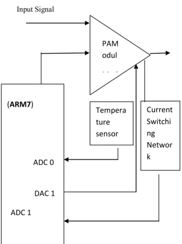
Flow Chart of Design Flow of Proposed Method Input signal Power amplifier module I to V convertor ADC OF ARM DAC OF ARM Control given to RF power amplifier module
2209 ISSN: 2278 – 7798 All Rights Reserved © 2014 IJSETR
Input Signal
Out signal
Fig 5. Block diagram oftest circuit
4.1 Temperature monitoring
The power amplifier’s power consumption influences its performance. The PA sometimes operates at a high quiescent point but at low output power. Lots of energy is wasted heating the devices under test, thus decreasing their reliability.Monitoring the PA temperature and adjusting its operating point can achieve best system performance. The temperature sensor is placed near to the power amplifier module whichdigitizes the values to the resolution
0.025°C. n ad the valued is given to the ADC of LPC2148 ARM7.
4.Hardwaredesign
The resetting module has been implemented differently in relation to the conventional method. The simplified block diagram of the simplified control system design is seen and discussed in design and implementation section.
Results of the application module indicate that the proposed system has performance considerations and safety and the control system with changes in temperature the affect over the threshold voltage is controlled using ARM processor.
The results of case temperature and the drain current are studied and it is found that the decreasing graph is obtained. Regulation of gate voltage so as the bias point is maintained and the respective voltages at the output of the system is observed and found to be controlled using DAC of LPC2148.Hence a controlled system with the bias voltage and temperature control due to rise in current of the circuit, the performance is carried satisfactorily.
4.2Development Tools
The Keil development tools offer numerous features and advantages that help you to develop embedded applications quickly and successfully. They are easy to use and are guaranteed to help you achieve your design goals in a timely manner. PAM odul Mod ule Current Switchi ng Networ k Tempera ture sensor (ARM7) ADC 0 DAC 1 ADC 1
2210 ISSN: 2278 – 7798 All Rights Reserved © 2014 IJSETR
Transimpedance amplifiers are commonly used in receivers for Optical communications to convert the current generated by a photodetector into a voltage signal for further amplification.
In this particular designed control system the output current from the power amplifier module is needed to be controlled hence it is given to the I to V converter so that the analog voltage value is given to ADC1 of ARM7 (LPC2148) and further digital conversions are performed using ARM7 and values are being compared with the values in the LUT and required adjustments are done using the DAC and the closed loop is formed for a control system.
5.Simulation Results
Results of the application module indicate that the proposed system has performance considerations and safety and the control system with changes in temperature the affect over the threshold voltage is controlled using ARM processor.
The results of case temperature and the drain current are studied and it is found that the decreasing graph is obtained. Regulation of gate voltage so as the bias point is maintained and the respective voltages at the output of the system is observed and found to be controlled using DAC of LPC2148. Hence a controlled system with the bias voltage and temperature control due to rise in current of the circuit, the performance is carried satisfactorily.
2211 ISSN: 2278 – 7798 All Rights Reserved © 2014 IJSETR
Lcd is connected to port 0 from pin no 16 to 23..in which 16 to 19 are data line connected to D4 to D7 pins of LCD and pin 20,21,22 is connected to control signal of LCD i.e En, R/W, C/D resptectively. LCD continuously display values of TEMP and CURRENT
GPIO—1 Simulation Window
LED is connected to pin 16 of port 1. This led is to indicate whether temp exceed the given threshold value,When this led turn on I to V operation comes into picture
Output Window1
The above fig shows the simulation window in keilµvision4 general purpose input output pins status is shown.i.e.GPIO 0 slow interface and GPIO 0 fast interface and the output of the ADC is shown by the A/D convertor 0 window selected
debugging. When the analog input is applied after the initialization of port 0The AD0 is applied with the input values to ADC and respective changes are being observed in A/D channel Data RESULT is shown
Output window 2
The above fig shows the description of the operation of the circuit when the temperature of the power amplifier exceeds the limit then the led at pin no. 16 of GPIO 0 fast interface becomes high as shown in GPIO window. And after this the analog data from the temperature monitoring unit is converted to DAC values which is shown at the DAC window, the
2212 ISSN: 2278 – 7798 All Rights Reserved © 2014 IJSETR
respective changes with the analog values from the A/D convertor the DAC window configures the DACR register and shows the value in DACR register and value and the respective analog value is shown.
Experimental Results
Values of Case Temperature and Drain
Current Id
6.CONCLUSION& FUTURE SCOPE
Controlling the gate temperature and current for RF power amplifier. Graphs are plot between the various die temperature and gate voltage and at various junction temperatures.Hence a control system with the use of ARM processor for power amplifier is made. With the different ways of gate voltage control system design and various affecting measures such as temperature and
current are found to be the sensitive parameters which are responsible for the hampering effect for an PA so among the available method the LUT (look up table) design using flash memory in ARM processor a feasible one and a system test design is made for an efficient monitor and a control system which can be useful for amplification in terms of power , current and with due effects of temperature on this technique with other multiuser software so that accuracy of result is maintained for better performances. Results of the application module indicate that the proposed system has performance considerations and safety and the control system with changes in temperature the affect over the threshold voltage is controlled using ARM processor.
Future Scope
In further study, it can be cut, expand and optimize the system, in order to make it more powerful. With the use of real time operating system so that the multitasking and sharing can be possible for an better efficient control system. In forthcoming efforts, analysis of different techniques by utilizing the circuit components with temperature compensation, to achieve the gate voltage compensation, but the gate voltage may not be independently regulated through this method. The other one is the using of SCM (single chip microcomputer) and memory storage of tables. In future one can explore the failure analysis of discrete components and integrated ones which tends to fail, causes major power losses for base stations. Hence the future work can be a better control technique using controlling algorithms for various readings for concluding the automatic control of gate voltage for RF PA amplifier to ensure high efficiency and linear work
Sr. No. case Temp id degree celsius current(ID in amp) 1 20 12 2 25 11.5 3 30 11 4 37 10.5 5 50 10 6 60 9.2 7 75 8.6 8 90 7.4 9 100 7
2213 ISSN: 2278 – 7798 All Rights Reserved © 2014 IJSETR
methodology self testing and correcting so further it can be implemented for various RF automatic applications
ABBREVATIONS:-
ADC- ANALOG-TO-DIGITAL CONVERTERS
ARM : ADVANCE RISK MACHINE
DACS:-DIGITAL-TO-ANALOG CONVERTERS GSM :-GLOBAL SYSTEM MOBILE
LDMOS :-LATERALLY DIFFUSED METAL-OXIDE SEMICONDUCTOR
LUT :-LOOK-UP TABLE PA :-POWER AMPLIFIER
QPSK :-QUADRATURE PHASE SHIFT KEYING
RTOS :-REAL TIME OPERATING SYSTEM SCM :-SINGLE CHIP MICROCOMPUTER UART: -UNIVERSAL ASYNCHRONOUS
RECEIVER & TRANSMISSION
ACKNOWLEDGMENT
I would like to take this opportunity to express my deep sense of gratitude to all who helped me directly or indirectly during this thesis work .First, I would like to thank my supervisor,
Mrs.PoojaThakre, for being a great mentor and
the best adviser I could ever have. Her advice, encouragement and critics are sources of innovative ideas, inspiration, and causes behind the successful completion of this dissertation. The confidence shown by her was the biggest
privilege working with her these past years
.
I am highly obliged to all the faculty members of Electronics Department for their support and encouragement. I would like to express my sincere appreciation and gratitude towards my friends at the institute,
especially, Mr. VijayPalaparthyetc, for their encouragement,
consistent support and invaluable suggestions at the time I needed the most. I am grateful to my family for their love, support and prayers
5. References
[1] Zhan sheng Zhang, Shuan long Pan. An adaptivegatevoltage control technology of LDMOS amplification device[J]. Mobile Communications, 2008, 32(24):58-61.
[2] Wei wei, Cheng. Research and realization of miniature intelligent linear Power Amplifier for
TD-SCDMA system [EB/OL].
http://10.22.2.78/kns50/detail.aspx?QueryID=4& CurRec=1.
[3] NeilZhao, MariahNie, NingJia. Analog Microcontroller Forms Heart of Low-Cost, High-Efficiency PA Monitor. Analog Dialogue. Volume 43 – March 2009
[4] HaoJianmin, Guo Kai, Cheng Hong, Ren Na. Design of Microoxidation power control system based on LPC2119. Electronic Measurement and Instruments, 2007.ICEMI '07.8th International Conference. 2007: 849 – 853.
[5] DaogangPeng, Hao Zhang, Kai Zhang, Hui Li, Fei Xia. Research and Development of the Remote I/O Data Acquisition System Based on Embedded
2214 ISSN: 2278 – 7798 All Rights Reserved © 2014 IJSETR
ARM Platform. 2009 International Conference on ElectronicComputer Technology. 2009:341-344.
Author profile
1]SnehaA.Dravyekar Mtech Pursuing
(VLSI)from Nagpur ,B.E.In Electronics Engg 2] Prof.PoojaThakreMtech (VLSI) Working as professor in Engineering college.
3]Prof.PraveshYadav Mtech (Electronics &Telecommunication) working as a Principal in Engineering college