Abstract—Hybrid electro-optical Network-on-Chip (HOE_
NoC) has recently been proposed to solve the problem of large scale interconnection. Although optical links in HOE_NoC provide high bandwidth and low latency for global communication, large static power consumed by laser and thermal tuning is also introduced. This leads to low power efficiency when the global traffic load is low. Anyway, for different application, traffic distribution in space and time may differ largely. It is necessary to dynamically provide optical link bandwidth to make the power efficiency keep high under all traffic distribution. In this paper, we propose a reconfigurable HOE_NoC architecture, in which, topology of electronic NoC is kept unchanged while the optical links can be reconfigured by dynamically throttling optical node. Experiments shown that compared to the electronic network under 64 nodes, latency has been reduced by 51%, while the throughput has been improved by 14%, the per-bit energy consumption has been reduced by about 26%.
Index Terms—hybrid, RHOE_NoC, reconfigurable
I. INTRODUCTION
ith the rapid development of semiconductor and integrated circuit technology, design of interconnection networks has become more challenging. Networks-on-Chip (NoC) technology has been used in various multi-core designs during past few years [1]–[2]. ENoC has the advantage of low latency in local communications but consumes higher power consumption and delay in global communication [3]–[4]. ONoC has better performance in global communications, however it shows bad performance for short-distance traffic and also consumes a lot of static power caused by laser source and micro-ring tuning [5]–[7].
Manuscript received July 2, 2018. This work was supported in part by the National Natural Science Foundation of China (No. 61774086, No. 61376025) and the Natural Science Foundation of Jiangsu Province (BK20160806).
Y. ZHANG is with the College of Electronic and Information Engineering, Nanjing University of Aeronautics and Astronautics, Nanjing, 211106, China. (Email: [email protected]).
N. WU is with the College of Electronic and Information Engineering, Nanjing University of Aeronautics and Astronautics, Nanjing, 210016, China. (Email: [email protected]).
F. GE is with the College of Electronic and Information Engineering, Nanjing University of Aeronautics and Astronautics, Nanjing, 210016, China.
G. YAN is with the College of Electronic and Information Engineering, Nanjing University of Aeronautics and Astronautics, Nanjing, 211106, China, and with the College of Mathematics, Physics and Information Engineering, Anhui Science and Technology University, Fengyang, 233100, China.
In order to fully exploit the bandwidth and power consumption advantages of optical links and preserve the high flexibility and low cost of electrical links, Hybrid optical-electrical NoC (HOE_NoC) has been proposed. Optical interconnects and electrical interconnects for global communications and local communications respectively, it is an effective solution for large-scale multi-core on-chip systems.
Ye et al. [8] has proposed a torus-based hierarchical optical-electronic NoC architecture THOE, which takes advantage of both electrical and optical routers and interconnects in a hierarchical manner. However, it limits the programing flexibility. Vantrease et al. [9] proposed a cluster-based optoelectronic hybrid topology. The network contains 256 IP cores divided into 64 clusters. The clusters are interconnected by devices within the cluster. Multiple-write-single-read (MWSR) optical bus network structures are used between clusters. Pan et al. [10] designed Firefly for 64 IP cores, which is divided into 16 clusters and each cluster is distributed in 4 groups. Four clusters with the same relative position are interconnected via separate optical bus networks depending on the relative position of the clusters within the group. These clustering structures aggregate nodes that are close to each other in a cluster and use electrical interconnects. In fact, the topological form of the clustering structure still has some potential problems in supporting local communications, fault tolerance and scalability of HOE_NoC.
The existing work has made a great contribution to the hybrid network. Our previous work [11] has proposed a novel non-cluster based hybrid electro-optical network architecture, in which topology of electronic NoC is maintained unchanged and an auxiliary optical NoC is built for the global communication speed up. Based on our observation, the accelerating network based HOE_NoC is essentially a rich-bandwidth design that helps increase the bandwidth and latency performance of many-core interconnect architectures, but it also brings the dual static energy consumption overhead of the opto-electrical links. Compared with the electrical interconnection network, which has large dynamic power consumption, the static power consumption generated by lasers and microring resonators tuning in the optical interconnection network is the main source of communication power consumption [12]. When the dynamic power consumption of the transmitted signal in the optical interconnection network is not sufficient to compensate for the static power consumption generated by it, the overall energy efficiency of the HOE_NoC system will be inferior to the all-electric interconnection network. In fact, there are
A Reconfigurable Hybrid Electro-optical
Network-on-Chip Architecture
Yafei Zhang, Ning Wu, Gaizhen Yan, Fen Ge
great differences in the spatial and temporal distribution characteristics of data communication under different many-core applications. The global communication and local communication requirements will also undergo major changes. The fixed optical interconnection bandwidth and supply will lead to underutilization of communication links under certain applications which is not conducive to improve the efficiency of the entire interconnect system. Therefore, it is necessary to design a reconfigurable HOE_NoC that provides the hardware basis for dynamically adjusting the optical interconnect bandwidth and the electrical interconnect bandwidth supply to improve the overall energy efficiency of the HOE_NoC.
Based on the above observation, we propose a reconfigurable based hybrid electro-optical network architecture (RHOE_NoC),which is an improvement to our previous work [12]. We keep the architecture unchanged and proposed a dynamically reconfigurable layout of optical nodes. It consists of an electrical interconnect layer and an optical interconnect layer. Each layer is connected through a 3D technology via TSVs. The electrical interconnect layer uses a conventional 2D Mesh to provide electrical connections for any two adjacent nodes. Since the number and layout of optical nodes have a great influence on the communication performance of the network, we use the Integer Linear Programming (ILP) method to optimize the number and placement of optical nodes to find the optimal solution.
The rest paper arranged as follows: Section II describes the proposed electro-optical NoC architecture and introduces the optimal placement method of optical node. Section III introduces nanophotonic crossbar implementation. Section IV shows dynamic reconfiguration scheme. In Section V, we present our experiment result and evaluate the performance of our proposed architecture. Section VI is the conclusion.
II. THEPROPOSEDRHOE_NOCANDOPTIMIZATION
A. RHOE_NoC Architecture Design
A proposed accelerating network based architecture of RHOE_NoC consists of 64 cores is shown in Fig.1. 64 cores are mapped on a 8×8 network. From Fig. 1(a) the bottom layer is the electrical interconnect layer (adjacent to the heat sink) and each tile contains a processor and an electrical router. The left inset shown in Fig. 1b illustrates an 8×8 Mesh. E-O Interface layer contains all of the photoelectric components (modulators, detectors) connected to the electrical interconnection layer via TSVs. The top layer is the optical interconnect layer which mainly consists of optical nodes and waveguides. The connection of the optical nodes is shown in Fig. 1(b) above.
Due to different applications, the global communication and local communication requirements have different spatio-temporal distribution characteristics. Communication load of each optical and electrical interconnection node have large differences. That leads to low utilization of the optical network that leads to more static power consumption. Therefore, in the case of different communication loads, it is necessary to dynamically reconfigure the optical nodes to
(c)
Processor Electronic router Electronic layer E-O Interface layer
Optical layer
Heat sink TSVs
(a)
(b)
Ring resonator
External Laser
TSV
0r 0g 0b 0y
2r 2g 2b 2y
3
r
3
g
3
b
3
y
1
r
1
g
1
b
1
y
modulators
d
et
ec
to
rs
detectors
d
et
ec
to
rs
Optical node 0
O
pt
ic
al
node
1
Optical node 2
O
pt
ic
al
node
[image:2.595.316.552.52.218.2]3
Fig. 1. Architecture of the proposed hybrid electro-optical NoC (a) Electrical die main consists of the processors, electrical routers, and TSVs to transmit signals between the two dies. The optical die contains the E-O Interface layer and an optical layer. (b) 3D architecture with the top inset showing the connection of the optical nodes and the left inset showing the8×8 Mesh.
reduce the power consumption of the network. RHOE_NoC topology design should follow the following principle:
(1) After an optical node is shut down due to a reconfiguration operation, its adjacent resource nodes can find alternative optical nodes for global communication and does not significantly increase the overhead incurred by optical interconnect global communications.
(2) The reconfiguration operation of a single optical node does not affect the network connectivity between other optical nodes.
(3) Minimize the impact of reconfiguration operations on the communication of resource nodes to avoid sharing of topological reconfiguration information in a wide range and reduce reconfiguration overhead.
B. The optimal placement method
To satisfy the design principle (1), it can be achieved by increasing the redundancy of the optical interconnect access points (optical interface unit) i.e. for any resource node at least rmin optical interconnect access points can be found
within hmax. The layout of the optical nodes of hmax=2 and
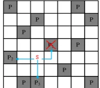
rmin=2 is shown in Fig.2. When the optical node P1 is closed
because of the reconfiguration operation, the resource node S can still find the optical node P2 and P3 for global
communication within 2 hops, and will not increase the additional overhead of the global communication of the surrounding resource nodes because of the closure of a single optical node. Since the layout and numbers of optical nodes have a great influence on the communication performance of the topology, we use the ILP method to solve the minimum number of optical nodes and the optimal layout under constraint conditions [13].
P P3 P
P
P2 S
P1 P
P
P P
P P
[image:2.595.379.483.676.767.2]1 2 3 4 5 6 7 8 57 25 41 33 17 9 49 59 27 43 35 19 11 51 60 28 44 36 20 12 52 61 29 45 37 21 13 53 63 31 47 39 23 15 55 62 30 46 38 22 14 54 58 26 42 34 18 10 50 64 32 48 40 24 16 56
Fig. 3. The nodes collection within 2 hops to node 36
The optimized layout should satisfy the following conditions:
(1) Within a specified number of hops, any resource node can find at least 2 optical interconnect access points.
(2) To ensure performance, number of optical nodes should be as small as possible.
(3) After the number of optical nodes is determined, number of optical nodes that each resource node accesses within a specified hop count is as many as possible.
A network can be regarded as consisting of a group of nodes N and links L which connect the nodes. The interconnection structure between the nodes defines the topology T = (N, L), which can be represented by the adjacency matrix A whose elements are defined as follows:
(
)
1
,
,
0
i j
ij i j
n n
L
a
n n
N
else
∈
=
,
∈
(1)If a direct connection between node ni and nj exists, the
corresponding element aij of adjacency matrix A is one,
otherwise, aij is zero. All nodes reachable by node ni within a
maximum Manhattan Distance of dmax are represented by the
index set Rdmax(i):
{
}
{
}
max max max1
0
0
d il liR
l
d
d
d
d
= ∈
| Ν | |
<
≤
∧ <
≤
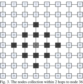
(2) As shown in the Fig. 3, we take node 36 as the optical node, then Rdmax(36)= {20, 27, 28, 29, 34, 35, 37, 38, 43, 44, 45, 52}.
In the electrical interconnect layer, we define two types of nodes: common nodes without an optical router (
S
⊆
N
) and nodes with an optical router (P
⊆
N
), an element Vi isone if the corresponding node i implements an optical router,
Vi=0 represents a common node. The minimal number kp of
required optical routers is obtained by the following optimization step:
{0 }
1
min
,
0
ip i i
i i
n
P
k
V
V
n
S
∈ |Ν|−1∈
=
=
∈
∑
(3) As a requirement, each common node shall reach a specified number of pillars. Thus, the optimization problem is subject to the constraint:{
}
( )
max
min
. .
1
h
m m R i
s t
i
V
r
∈
∀ ∈
| Ν |
∑
≥
(4)P
+1 +1P
+1 +1P
+1 +1 +1+1 +1
P P
+1 +1+1 +1 +1
P
P
P
P
+1P
+1 +1 +1+1 +1 +2
P
+2
P
+1 +1 +1+1 +1 +1
P
+2P
+2 +1 +1+1 +1 +1
P
+1
P
(a) Unoptimized (b) Optimized Fig. 4. Minimal placements with and without redundancy optimization
The above model only solves the minimum number of optical nodes required by the network and does not consider optimizing the layout of the optical nodes. We define the redundancy of a network as the sum of redundancies redi of all
nodes. In the case of the same kp, different layout schemes
may provide different redundancy, as shown in Fig.4, optimized layout has bigger redundancy. However, the bigger redundant network has better communication performance. To find the placement providing the maximal redundancy for a given kp, the maximum redundancy kr is obtained by the
following optimization step: {1 }
max
r i ik
red
∈ |Ν|=
∑
(5)kp is the result of the first optimization, there are
constraints:
{1 }
i p i
V
k
∈ |Ν|=
∑
(6) The redundancy redi is the number of optical nodes inRdmax(i), to prevent optical nodes placed next to each other as
far as possible, their redundancy redi is accounted to zero.
{
}
(
)
( )
max
1
1
h
i i j
j R i
i
red
V
V
∈
∀ ∈
| Ν |
= −
∑
(7)The redundancy redi of each node has to satisfy at least
minimal number of optical nodes given by rmin.
{
1
}
i(
1
i)
mini
red
V r
∀ ∈
| Ν |
≥ −
(8)We set hmax =2 and rmin =2, i.e. every node can find at least
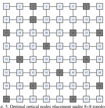
two optical routers within two hops. CPLEX, ILP software solver, is utilized to find the minimized count and maximized redundant optical routers. The optimal layout of the optical nodes in 8×8 mesh network is shown in Fig.5.
Based on this scheme, a reconfigurable architecture under 8×8 mesh topology RHOE_NoC is shown in Fig.6. Global traffic will be firstly sent to the nearest node with optical interface and then be delivered in the optical link.
1 2 3 4 5 6 7 8
57 25
41 33 17 9
49
59 27
43 35 19 11
51
60 28
44 36 20 12
52
61 29
45 37 21 13
53
63 31
47 39 23 15
55
62 30
46 38 22 14
54
58 26
42 34 18 10
50
64 32
48 40 24 16
56
Fig. 5. Optimal optical nodes placement under 8×8 topology
s
D
S Source node
D Destination node Electronic path Optical path
Fig. 6. The optimal architecture of RHOE-NoC
by default. When the optical node needs to send a data packet, first, the transmitter broadcasts a reservation signal including the destination node and the packet length information to all the detectors on the waveguide and then only the destination optical node will allow corresponding detector to receive data for respective data channel. Based on the SWMR optical cross-switch, all optical nodes are one-hop communication. Therefore, when a single optical node is reconfigured to be closed by activation, it will not affect the communication of other optical nodes.
Point 0 Point 1 Point N-1 CH0a CH1a CH(N-1)a
CH0 CH1
CH(N-1)
… …
… … … …
…
… …
… …
…
… …
… Cont
rol
Ne
two
rk
D
ata
Ne
two
[image:4.595.82.264.55.243.2]rk
Fig. 7. Reservation-assisted SWMR (R-SWMR)
When the transmitter is reconfigured, it only needs to share the reconfiguration information among resource nodes in its communication domain. According to whether the optical nodes are in their communication domain are closed, each resource node dynamically decides which communication nodes in the communication domain to carry out global communication. When the detector is reconfigured, it is only necessary to share the reconfiguration information among the resource nodes in its communication domain. After the nodes receive the topology reconfiguration information, the request is initiated to the nearest light node through the domain and the global communication for the target node will be received and forwarded through the adjacent light nodes. Both
[image:4.595.340.509.92.188.2]transmitter and detector reconfiguration can avoid topological information sharing in the whole network.
TABLE I
SIMULATION PARAMETER Topology Size 64 nodes
Buffer Depth 16 flits Flit Width 128 bit Packet Size 4 flits ONI Buffer 32 flits Clock Frequency 2.5 GHz Optical Baud Rate 10 Gbps Traffic Model Random Simulation Time 5000 cycles
IV. DYNAMICRECONFIGURATIONSCHEME The dynamic reconfiguration scheme of optical node performs a reconfiguration operation according to the load state of the optical interconnect node. Based on the network link utilization and average buffer utilization, we propose a dynamic reconfiguration logic algorithm as shown in the Table II.
TABLEII
RECONFIGURATION ALGORITHM Step1: Wait for Reconfiguration window, W
Step2: For all optical nodes i, each hardware counter calculate Li
u and Biu in the current W and sends data to reconfiguration controller(RC)
Step3: Each RCi performs load determination and reconfiguration decisions:
If Liu < Lu(low)
Turn off the corresponding optical node If Lu(low) ≤ Liu ≤ Lu(congest) and Biu ≤ Bu(congest) Without reconfiguration
If Biu > Bu(congest)
Open adjacent optical nodes that were closed Step4: The reconfigured optical node sends topology
reconfiguration information to all nodes in its communication domain. After receiving the message, each node initiates a join request to its nearest optical node communication domain.
Step5: Reconfiguration completed, goto Step 1
V. EXPERIMENTANDRESULT
We implement three networks: mesh based electronic network (E_Mesh), non-cluster hybrid electro-optical network (HEO_NC) and our reconfigurable hybrid electro-optical network (RHOE_NoC) in the cycle-accurate network simulation environment of JADE [15]. Average latency, throughput and power efficiency of each network have been evaluated and compared according to following simulation parameter listed in Table I.
A. Latency
Latency comparison result under 64 nodes topology size is shown in Fig.8. It is observed that, as compared to E_Mesh network latency of the proposed RHOE_NoC has been greatly reduced, at most 51% reduction has been observed. HEO_NC has better performance than RHOE_NoC, at most 54% reduction has been observed. That is for global communication, HEO_NC can find optical node within one hop but RHOE_NoC may need two hops, which increase the delay of electric network communication.
B. Throughput
[image:4.595.56.282.492.608.2]topology size are shown in Fig.9. E_Mesh get saturated at the packet injection point of 0.35. The proposed RHOE_NoC has extends the point to 0.4. Further the saturation throughput has been improved by 14%, compared to E_Mesh under the same topology size. HEO_NC has the best performance among the three networks because HEO_NC has more optical nodes than RHOE_NoC.
C. Energy Efficiency
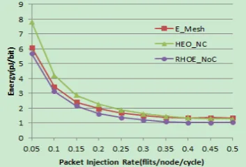
Energy efficiency comparison result under 64 nodes topology size shown in Fig.10. Compared to the E_Mesh network, the proposed RHOE_NoC has reduced the energy consumption by about 26% when the network load gets saturated, and much better than HEO_NC. Due to optical links incur large static power consumption, HEO_NC shows low power efficiency when the network load is light, even worse than E_Mesh.
[image:5.595.79.266.342.739.2]Although HEO_NC shows excellent latency and throughput performance, power efficiency of HEO_NC is extremely worse than RHOE_NoC. It is shown that optical network can produce huge static power consumption, even for low channel utilization. Since, RHOE_NoC can reduce the static power by dynamically reconfigurating the optical nodes, it has the best power efficiency performance.
[image:5.595.89.262.344.457.2]Fig. 8.Latency under 64 nodes network
Fig. 9.Throughput under 64 nodes network
Fig. 10.Energy efficiency under 64 nodes network
VI. CONCLUSION
In this paper, we present a reconfigurable based electro-optical hybrid NoC architecture, in which electrical interconnection is kept between any two nodes and optical links are provided to accelerate the long distance packets delivering. Above all, RHOE_NoC can dynamically reconfigurate optical nodes to adapt to different applications. Experiments show that our proposed reconfigurable hybrid NoC architecture is beneficial to the system throughput, latency and power efficiency. In particular, it can reduce a large number of static power consumption.
VII. REFERENCES
[1] A. Agarwal, C. Iskander and R. Shankar, “Survey of Network onChip (NoC) Architectures and Contributions,” Journal of Engineering, Computing & Architecture, Vol. 3, No. 1, 2009
[2] Masoud Oveis Gharan and Gul N. Khan, “Flexible simulation and modeling for 2D topology NoC system design,” in proc. IEEE Electrical and Computer Engineering, pp. 180–185, 2011.
[3] J. Owens, “Research challenges for on-chip interconnection networks,” Micro, vol. 27, no. 5, pp. 96–108, 2007.
[4] R. G. Beausoleil, P. J. Kuekes, G. S. Snider, S.-H. Wang, and R. S. Williams, “Nanoelectronic and nanophotonic interconnect,” Proceedings of the IEEE, 2008.
[5] Cho. H, Kapur. P , and Saraswat. K, “Power comparison between high-speed electrical and optical interconnects for inter-chip communication,” In Proceedings of the IEEE International In- terconnect Technology Conference (IITC), pp: 116–118, 2004. [6] Young. I, Mohammed. E, Liao. J, Kern. A, Palermo. S, Block. B,
Reshotko. M, and Chang. P, “Optical I/O technology for tera-scale computing,” In Proceedings of the IEEE International Solid-State Circuits Conference (ISSCC), pp: 468–469, 2009.
[7] Parisa Khadem Hamedani, Natalie Enright Jerger and Shaahin Hessabi, “QuT: A Low-Power Optical Network-on-Chip,” Eighth IEEE/ACM International Symposium on Networks-on-Chip (NoCS), pp. 80-87, 2014.
[8] Yaoyao Ye, Jiang Xu, Xiaowen Wu, Wei Zhang, Weichen Liu, Mahdi Nikdast, “A Torus-based Hierarchical Optical-Electronic Network-on-Chip for Multiprocessor System-on-Chip,” ACM Journal on Emerging Technologies in Computing Systems, vol. 8, no 1, February 2012.
[9] Dana Vantrease, Robert Schreiber, Matteo Monchiero, Moray McLaren, Norman P. Jouppi, Marco Fiorentino, Al Davis, “Corona: System Implications of Emerging Nanophotonic Technology,” 35th International Symposium on Computer Architecture, ISCA, pp. 153 – 164, 2008.
[10] Y. Pan, P. Kumar, J. Kim, G. Memik, Y. Zhang, and A. Choudhary,
“Firefly: Illuminating future network-on-chip with nanophotonics,” in Proc. 36th ISCA, pp. 429–440, 2009.
[11] Yan G, Wu N, Zhou Z. A Novel Non-cluster based architecture of hybrid electro-optical Network-on-Chip[J]. Iaeng International Journal of Computer Science, 2017, 44(3):368-374.
[12] R. K. Dokania and A. B. Apsel, “Analysis of Challenges for On-Chip Optical Interconnects,” In Proceedings of the 19th ACM Great Lakes symposium on VLSI, pp. 275-280, 2009.
[13] Xu T C, Schley G, Liljeberg P, et al. Optimal placement of vertical connections in 3D Network-on-Chip[J]. Journal of Systems Architecture the Euromicro Journal, 2013, 59(7):441-454.
[14] Christoforos Kachris. Photonic Network-on-Chip Design[J]. Integrated Circuits & Systems, pp. 173-178, 2013, 68.
[image:5.595.80.257.625.745.2]